I own a 100 Watt rack mount Traynor (PA system) amp that I've used for years. I'm thinking of building two just like it for a project. In looking at the design, there's something that I haven't been able to figure out what it's for. I first thought it might be an error on the drawing, but in looking at the amp, it is indeed there.
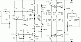
I understand the circuit around the 2N6553 is a current sink, but what in the world does the zenor (1N4745 going to ground) in series with the 22MF cap do? Is it some kind of limiting circuit? I've not seen anything quite like this before.
I understand the circuit around the 2N6553 is a current sink, but what in the world does the zenor (1N4745 going to ground) in series with the 22MF cap do? Is it some kind of limiting circuit? I've not seen anything quite like this before.
Attachments
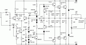
It looks like this amplifier has no relay based protection circuit that delays loudspeaker connection to amplifier after powering it up. Usually without that circuit there is uncontrollable DC pulse applied to the speaker duration of which depends on time costants of current sources.
In that circuit diodes of current source are immediately biased by charge current which flows via zener diode and capacitor in series. This capacitor limits the current. This way capacitor in parallel to diodes is being charged much faster then via 33kOhm resistor to the ground. After that DC biasing current is determined only by 33k resistor.
It limits duration and amplitude of the click in the speaker.
There is at least one major error in the circuit, but setting
that aside, IMHO the current source biasing for the front end
diff pair and VAS is not very good, and the circuit you ask about
appears to be an effort to patch it. I suggest you borrow
a current source design from another amplifier.
that aside, IMHO the current source biasing for the front end
diff pair and VAS is not very good, and the circuit you ask about
appears to be an effort to patch it. I suggest you borrow
a current source design from another amplifier.
It might be worth your while to review the entire schematic against the actual circuit before attempting to build more amps like it. If the schematic doesn't agree with the physical circuit, then scribble in corrections.
Grey
Grey
It looks like a deglitcher to keep the CCS transistor out of cutoff while the 22uF capacitors charge up. The zener has a V(z) of 16V, and has 43.6V between that point and ground. It looks like a hack to correct some problem they had with adding those capacitors to the CCS there. However, that isn't what concerns me about this. See #1 of attached schematic: that capacitor has the wrong polarity.  That is just asking for trouble, even if the voltage across is just 1.4V.
That is just asking for trouble, even if the voltage across is just 1.4V.Attachments
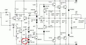
Miles Prower said:.....even if the voltage across is just 1.4V...
I'ts just 0,7V. The emitter resistor is missing.
VAS CCS doesn't work.
I don't know where that schematic came from, and didn't bother to check past that backwards capacitor to see if the CCS transistor was an internal Darlington or not. If it isn't, then that missing emitter resistor will, indeed, cause it to go into hard saturation and cease to function as a CCS anyway. Makes me wonder if that isn't a sample schematic from a kit. These are often deliberately wrong so as to result in a non-functional circuit so that you will be forced to buy the kit to get the correct design.
Still, WTF are all those capacitors doing down there anyway? I did a solid state design and didn't have a single one in any CCS in that design.
Still, WTF are all those capacitors doing down there anyway?
I did a solid state design and didn't have a single one in any CCS in that design.I went back and looked at the schematic and my hand drawings from the actual amp and found two big errors on my drawing!
The polarity of the cap in question was indeed wrong, and I left out the emitter resistor. I have gone back through the drawing and believe this is now correct.
The amp does not have any kind of relay power on/off pulse protection. I agree the zener and cap are probably an attempt to limit that. I intend to add relay protection if I build any of these. I also wonder if making the bias adjustable would be a good idea.
The amp works pretty well, but if anyone has one around 100 watts that would be better, I'd appreciate seeing the schematic.
Here is the corrected drawing:
Attachments
Hi Brion,
glad I came in late - you sure you have the drawing right?
The 22MF on the input tail current source as a filter is doing the wrong thing! REMOVE IT
The 16V Zener and 22MF you speak of REMOVE BOTH.
The 15pF should be on the Vas not it's current source. It needs a source impedance - not two diodes. MOVE IT
The input stage RC comp (series 1n5, 470R) is useless for a single ended output. You can move it to across the 2K2 that's feeding the Vas or probably LEAVE IT OUT.
CHANGES
Take the base of your BC550 current source to the top of the two diodes for the Vas current source and change the emitter 15K to 560R . Put a 2K2 between the same diodes and the Vas CCs base with a 22MF to the neg supply - that will do the dethump. Change the emitter resistor to roughly 56R - should give more symm clipping and slightly lower THD.
For starters.
Cheers,
Greg
Greg et al,
I often wondered why this amp seemed more complicated than it needed to be. I won't change the original Traynor amp as it works fine (even with the extra junk), but I appreciate the help with designing something better and less complicated that I can build for my project.
I think this drawing accurately reflects the changes you have suggested. It certainly simplifies the design, and makes it look like many other amplifiers I have schematics for. If you see any other glaring errors (or even some that aren't so glaring) please let me know.
Thank you all!
Attachments
Hi Brion,
Close but not quite. The first stage tail constant current source emitter resistor shown as 56R -> 560R.
The protection cct could do with some improvement as it's just a 5A per device current limit, irrespective of Vout level.
You may wish to increase the input and feedback (and associated R's) as 4K7 is very low input impedance. I would use 10K as a bare minimum and the 180 -> 390.
Cheers,
Greg
Brion55 said:I went back and looked at the schematic and my hand drawings from the actual amp and found two big errors on my drawing!
You might want to draw the MPSA56 current limiter as a PNP.
😎
Interestingly, the original Tryanor schematic shows the MPSA56 as an NPN! Guess you can't even trust Mfg schematics to be correct.
One more time:
Gosh, there is a "0" in 560R... oops!
Made the R changes suggested. I assumed the 47pf in the NFB circuit needed to be reduced by the same amount the voltage divider R's were increased (X3). Correct?
I added a trimpot for bias adjust (nice to have). Would it be that much better to have a "servo" type of bias circuit with transistor mounted on the output Q's heatsink for better temp stability?
Getting closer?
Attachments
Hi Brion,
you have changed to Miller compensation. Why?
Put your comp cap back to the inverting base and add in space to put in a parallel RC from VAS collector to inverting base. Also add in a location for an RC in parallel to the LTP load ie. +Vrail to VAS base.
you have changed to Miller compensation. Why?
Put your comp cap back to the inverting base and add in space to put in a parallel RC from VAS collector to inverting base. Also add in a location for an RC in parallel to the LTP load ie. +Vrail to VAS base.
Yes Andrew T's right - the 47p from Vas collector to feedback point needs to go back in.
Yes a Vbe multiplier would be better as it represents better the number of diodes in the output stage for tempco ( but ignores the Vas tempco) but should go closer than 2-3 diodes +Rtrim.
Andrew T,
the RC comp on the input stage appears to do nothing as standard so is likely not needed at all.
Cheers,
Greg
I assume that since the NFB voltage divider was changed the 47PF you want me to put back in needs to be changed to reflect that?
How's this for a servo bias?
Again, thanks for your help. I'm pretty good with tube amp design but haven't had much experience with SS.
How's this for a servo bias?
Again, thanks for your help. I'm pretty good with tube amp design but haven't had much experience with SS.
Attachments
what about adding degeneration resistors to the long tailed pair,
from about 47 to 100 ohm?
rgrds,
hienrich😀
from about 47 to 100 ohm?
rgrds,
hienrich😀
I would:
1. Remove the 2K2 collector load on the inverting input Transistor. Not required, has no effect on balanced current.
2. Insert another 2K2/22uF decoupler on the base of the LTP CCS. This prevents any output modulation of the rail producing current artefacts in the input stage.
3. Remove the cap bypass on the fb resistor, and re-install a small but finite lag comp cap across the base/collector of the VAS. Somewhere around 47pF should do it. Local VAS lag compensation gets a bad rap, but it is the most influential means yet of guaranteeing cast iron stability WITH good sonics. I have seen fb resistor bypass caps do very unpredictable things........
Cheers,
Hugh
Hugh,
Someone else told me to take the cap from VAS C-B out! I'm getting conflicting advice and not sure what to do.
What about the 15pf from VAS collector to FB point? Does that stay too?
Someone else told me to take the cap from VAS C-B out! I'm getting conflicting advice and not sure what to do.
What about the 15pf from VAS collector to FB point? Does that stay too?
Brion,
Welcome to hifi!! You will always have conflicting opinions from experts - that's why they are experts, they all march to a different step...... you must select one you think could be right, follow his advice, build it, verify it one way or the other, and either accept or discount that advice. If it's wrong, try another..... until you find someone who really knows his stuff.
A very good way to do this is to read the history of amplifier development, starting with Black, the discoverer of Negative Feedback in the twenties.
I stand by my earlier advice, with both lag comp AND phase lead caps. However, only you can figure out if it's good advice. You have to build it, listen to it, assess it. That takes a lot more effort than drawing a schematic, and a few dollars as well. If you are serious about designing an amp, you don't have any other alternative. Build it. Listen to it. Form opinions based on something other than PSpice....... It's a rewarding journey, but it's long and demanding. This is no sprint!
Cheers,
Hugh
- Status
- Not open for further replies.
- Home
- Amplifiers
- Solid State
- Calling all amp theory gurus