I'm new to circuit design and trying to read and learn a lot, but almost every calculation for common emitter amp circuit components is slightly different. I understand that there are many variables in this circuit, but all these different methods just giving me more confusion.
What would be the right way to calculate Rc and Rc out of these:
Calculating the Collector Resistor (Rc):
Version 1: Rc = Vcquiescent / Icquiescent = (Vcc / 2) / (Ic / 2). So here we have a maximum collector current (Saturation). We want the quiescent current to be somewhere in the middle, halfway of Ic and use that to calculate Rc. This doesn't make much sense to me as in this case Icquiescent becomes Ic as the resistor will determine the maximum current as Icquiescent.
Version 2: Rc = Vcquiescent / Ic = (Vcc / 2) / Ic. Using maximum collector current. (Saturation)
Calculating the Emitter Resistor (Re):
Version 1: Re = Ve / Icquiescent = (Vcc / 10) / (Ic / 2). Using the quiescent collector current to calculate Re. Ve is chosen to be one tenth of Vcc. We also assume Ie is same as Ic.
Version 2: Re = Ve / Ic = (Vcc / 10) / Ic. In this case we use the maximum collector current available at saturation.
Yes, there are a number of ways to do this. This is a good explanation.
https://www.instructables.com/How-to-Design-Common-Emitter-Amplifier/
https://www.instructables.com/How-to-Design-Common-Emitter-Amplifier/

Thanks Rayma. I read through this before and what I don't understand yet is that why they start off with 1 amp if the resistor will determine the maximum collector current as 0.5A? It seems like they use Icquiescent to calculate Rc instead of Ic, so the collector current can never go over 0.5 amps. Please correct me if I'm wrong here.
On second thought that is not such a great discussion. Here's one that looks more practical.
https://electronics.stackexchange.c...erstanding-the-basic-common-emitter-amplifier
The Q point (DC collector voltage and current) is often chosen at around half the supply DC voltage,
so the AC signal swing at the collector can be more or less symmetrical.
The DC collector current can be chosen on the basis of several factors: low current for battery use;
maximizing beta; driving the necessary load; distortion, etc. Often 1mA works ok for higher impedance loads.
About 1mA bias current would be needed to drive a 1k load to 1V peak., for example.
The AC voltage gain will usually be around a factor of Rc / Re for typical designs,
unless the Re is bypassed with a capacitor for somewhat higher gain, but also higher distortion.
The maximum peak output current will be somewhat less than the DC bias current.
Plotting a load line can help visualize the signal swing for the chosen Q point.
If you could give some specifications for the required output voltage, load resistance, voltage gain, frequency response, and input resistance for that amplifier stage as a "black box," I could do a generalized design that could be extrapolated to other specs. This might be of some value to the community. The internet is awash in stuff that is just plain wrong or not very generalizable.
Glad to help out
Glad to help out
I put together an amp and tweaked the values, so we could start from there.
Frequency response should be the usual 20 - 20 kHz range, input impedance, high enough to connect it directly to headphone output. Can't give specific values, as I'm just learning this stuff and my knowledge is very limited yet. I'm trying to achieve as much gain as possible. So I calculated component values I needed, tried it in LTspice, then I put together the physical components and checked the output and tweaked the resistor values. What surprised me is that when I test the actual amplifier, I don't get any distortion for example even at 5Vpp but when I look at LTspice my circuit starts to distort even at 0.4Vpp and not sure why there's a huge difference compared to real life testing. The amp sounds excellent till about 75% volume of my DAC headphones output, then it starts to distort slightly especially with bass heavy music. Volume before distortion is quite good, but I'm planning to change the design to get more power output. Currently the amplifier draws 1.25A at 30Vcc. I'm planning to raise the voltage to 50 volts so I can have a larger ratio between the collector and the emitter resistors and hopefully increase gain. Please see my Spice circuit plan below. Those are the experimented real life values. I'm curious why test results between Spice and the actual amp are so different and if you would change any of those values. I'd also like to know what you think about increasing the voltage (and values) to get some more undistorted volume, assuming the output capacitor is big enough.
PS: I changed BF of the transistor in the model to 75 according to the graph at 2A Ic(quiescent).
Attachments
Last edited:
With a bypassed emitter resistor, the input resistance of the amplifier is very small, being only a few ohms. What were you using to supply the signal in your hardware test? Did you check distortion using the FFT, or LTSPICE "measure" command? One common definition of distortion limits for stages like this is the limit of ic (The ac signal current in the collector) should be less than ICQ x 0.2. This results in a second harmonic amplitude of 10% of the fundamental amplitude. I have measured this in the lab many times, and it is reasonably accurate, derived from the basic definitions of BJT operation, i.e., transconductance and the incremental resistance of the forward-biased base-emitter junction. For example, if the quiescent collector current is 1 A, then the collector current should range from 0.8 amps to 1.2 amps under maximum signal conditions. Note that distortion in the frequency domain is measurable long before you see it in the time domain, meaning on the scope.
Here is an old trick for getting a quick idea of distortion when using a scope, and it gives you a notion of second harmonic distortion components. Center your scope sweep at 0 volts before applying the signal. The measure the positive and negative peaks of the waveform. If there is no distortion, then the magnitude of the peaks should be equal. If they are different, say +3.1V and -2.9V, then second harmonics are present. Once you see clipping, it is way too late!
Are you trying to drive speakers with circuit?
Thanks for the tips about spotting harmonics, as my Rigol which had FTT function had a fault and I had to return it so I'm stuck with a cheap pocket oscilloscope from eBay, which is fine to visualize the wave form, and spot bigger distortions, but like you said by then the problem is probably way bigger.
Yes, I tried to drive speakers, but in the past few days I managed to learn a few things and realised, that I would be better off having a common emitter amplifier as a preamp and connect a common collector one as the output stage. So the CC one will get enough voltage swing and the CE doesn't have to drive a speaker.
I remember the magnitude difference in Spice, but I will try to use the measure command to get exact values when I see it happening again.
So to return to the initial question, to calculate Rc I would choose a collector current (which would be large enough to drive my common collector output stage), then divide half the supply voltage with it: Version 2: Rc = Vcquiescent / Ic = (Vcc / 2) / Ic.
For Re it seems right to take one tenth of Vcc and divide it by the quiescent collector current, which is half of Ic that we used for Rc: Version 1: Re = Ve / Icquiescent = (Vcc / 10) / (Ic / 2)
Would you do it the same way?
You are correct to make it a 2 stage design, with a CE stage driving a CC stage. With a little careful though, you can make it a direct-coupled design and simplify the biasing.
The first step is to set up a few specs. What voltage swing are you trying to produce in the 8-ohm load? You need that first to complete the rest of the design. After that, we can work through it step by step.
The first step is to set up a few specs. What voltage swing are you trying to produce in the 8-ohm load? You need that first to complete the rest of the design. After that, we can work through it step by step.
What model headphones? Headphone impedance tends to vary quite a bit, but I've seen something like 8 ohms to 300 ohms. The lower the impedance, the lower the voltage needed but the higher the current needed. Regardless, this could take significant power from the transistor and load resistor, and you may need to account for that as well as resistances, voltages and currents.I put together an amp and tweaked the values, so we could start from there.
Frequency response should be the usual 20 - 20 kHz range, input impedance, high enough to connect it directly to headphone output. Can't give specific values, as I'm just learning this stuff and my knowledge is very limited yet.
I see you've decided to add a buffer stage, but to find the answer to the discrepancy between Spice and real life, stay with your original circuit for a minute.
First, measure the voltage at the output of your DAC and amp at the level before you hear distortion. Is it really 1 volt? If so, you should be clipping hard. Common emitter gain is -RC/RE, the ratio of resistance in the collector circuit to resistance in the emitter circuit. You're AC bypassing the emitter resistor, so all that's left is intrinsic emitter resistance (re), equal to VT/IC. At room temperature, VT~26mV, and 32mV at 100degC. Your load resistance is 8R||16.5R=5.4R. With IC approximately 1A, that gives 5.4/.026=208. With a 1V input, you get 208V output.
As a result, your circuit clips in Spice. To better understand what your simulated amp is doing, plot collector current rather than the resistor current.
A few other notes:
-You'll often see the gain equation listed as gmRL. gm is the inverse of re.
-You haven't modeled the output impedance of your DAC in Spice. If driving a high impedance you'd probably get close enough results without doing so, but as mentioned by @LVQ, you're driving a low impedance. So your DAC could put out 1V into a typical load but much less into the amp you built.
-Input resistance of a BJT = rbb(parasitic base resistance)+beta*RE. With no degeneration, RE becomes re, and for a power transistor, rbb is usually low. In Spice, rbb is RB at low currents, and transitions to RBM at high currents, with IRB the current where it's halfway between the two. For your circuit, the BJT input impedance is in parallel with the two base bias resistors.
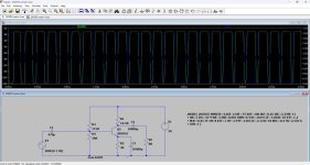
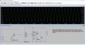
Thanks for the very useful notes @dkfan9 and I'm going to come back to this and to @benb 's comment as well, but like @LVQ suggested I need to start the full design at the other end, which is the output stage. So to answer the question about the voltage swing into 8 ohms, I came up with the following design. I'd love to say I calculated all those values, but half of it was tinkering until I got it right. So I biased the base at 15.7 volts to account for the voltage drop across the base-emitter junction. (Vb brown line in graph). This gives me an emitter voltage of 15 volts (red line) and an emitter quiescent current of approximately 1 amp when no signal connected. As you can see below, everything works fine until 10Vpp, but at 14Vpp there is clipping. As I understand, this is because the voltage of the capacitor is equal or higher than the emitter voltage, so the base-emitter junction cuts off.
At this point I need to make a choice how to carry on. Currently the only way I know this issue can be eliminated is to use another transistor (PNP + NPN, push-pull arrangement) to help sinking the current that doesn't have time to sink through the speaker. If there are other ways, maybe someone can tell. (Reducing the coupling capacitance or reducing Re didn't help)
As my original plan is to build a single-ended amp first, I'd like to stick with it for now if that's possible. It looks like it would work as long as I stay below 10V peak to peak at the input.
PS.: I didn't include the possible output impedance of a preamp stage, this might be a problem, but not too sure.
Last edited:
- Home
- Amplifiers
- Solid State
- Calculating Rc and Re in a Common Emitter Amplifier circuit