Hello crazy people. I've built a chip amp once, but not exactly for audio. I am now building my first audio amplifier, for use as the amplifier in the "monitor" system of the computers my friends who work with music and movies use. The idea is just making something for them to use instead of headphones, and instead of those crappy 0.25W "multimedia" speakers.
I selected the TDA2007 because it is the chip from the family that seems to be better suited for this task, i.e. has the perfect power rating. It seems to be kind of old, tough, and the example board is very ugly.
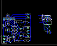
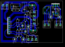
I would appreciate to have some feedback from you as I develop this project. I am sending attached images from my Eagle project for the board. I tried to redesign the PCB, and comments on my design would be much appreciated. I also have to design the PSU, and advice there would also help. I am thinking about using a LM350 regulator after a full wave rectifier. I still have to select the transformer, or decide to use a solid-state PSU instead.
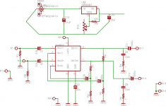
The source voltage should be 22V, like the datasheet suggests (8 Ohms speakers). The only difference of this circuit from the datasheet is that I took off the source capacitors, and selected 1000 uF caps at the signal output.
So, do you have any advices about changes I should do to the datasheet circuit? And what about my new PCB, is it looking good?
cheers,
++nic
I selected the TDA2007 because it is the chip from the family that seems to be better suited for this task, i.e. has the perfect power rating. It seems to be kind of old, tough, and the example board is very ugly.
I would appreciate to have some feedback from you as I develop this project. I am sending attached images from my Eagle project for the board. I tried to redesign the PCB, and comments on my design would be much appreciated. I also have to design the PSU, and advice there would also help. I am thinking about using a LM350 regulator after a full wave rectifier. I still have to select the transformer, or decide to use a solid-state PSU instead.
The source voltage should be 22V, like the datasheet suggests (8 Ohms speakers). The only difference of this circuit from the datasheet is that I took off the source capacitors, and selected 1000 uF caps at the signal output.
So, do you have any advices about changes I should do to the datasheet circuit? And what about my new PCB, is it looking good?
cheers,
++nic
Attachments
With such an IC a regulated power supply is difficult to justify. It is more complex, more expensive and wastes energy. An unregulated supply would be more consistent with the price and quality of the TDA2007.
If you use a voltage regulator, there are a few hints that you can get from the datasheet. At the input a 0,1 µF capacitor is only suitable, if it is a ceramic or MKP type. A tantalum should be 1 µF and a normal electrolytic should be at least 25 µF. The same goes for the output. A bigger smoothing capacitor between rectifier and input would not hurt either.
Tip: don't go for tantalum capacitors. They have good electrical properties, especially at high frequencies, but they are the only capacitors that tend to fail on their own. They produce internal shorts and can even blow up, when they fail.
It is recommendable to use a protection diode from output to input of the regulator.
Replace the trimmer with a multi-turn type (e. g. 64W), otherwise voltage adjusting will be tedious.
Don't forget the heatsink for the regulator. The TO-220 will have something like 50 to 60 K/W junction to air. Assuming that your supply voltage is at an average 5 V above the regulated voltage and a peak current of 1,5 A you get 7,5 W of power dissipation. 7,5 * 50 = 375 K. Add 25 °C ambient to that and you get 400 °C junction temperature, where 125 °C is the allowed maximum.
Capacitors don't like heat. In your layout C3 is right by the TDA's heatsinking surface. Try to move it somewhere else. C12 and C13 are right by the LM350, which will also become hot. Move them away from there. Especially C12 must leave space for the heatsink. And C6 and C8 could use a few millimeters more distance to the TDA as well.
The datasheet layout has the advantage that it does not need a jumper like yours. In a new design, one should probably try to make a star-shaped ground with the star-point next to the input ground connection instead of a ground fence around the PCB.
I agree with pacificblue, lose the regulator and put in some large caps for the voltage rail, such as a 2200uF 25V or 35V just to be safe. 😉
Another option would be a pair of TDA1905's which are 5W mono chips in a POWERDIP16 package. http://www.datasheetcatalog.org/datasheet/stmicroelectronics/1446.pdf
I still have around 400+ of these in their antistatic tubes 'cause there was a sale on at some store a few years back. Great for little speaker projects for friends. ^_^
Hi, guys. Thanks for all the tips.
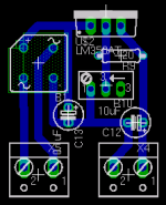
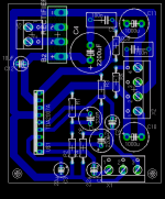
I am thinking about testing it without the regulator also, and just a rectifier with large caps instead. That's why I am building the PSU separately... I updated the board design for it (attached). I left the protection diode out because the datasheet said it was only strictly necessary ate larger voltages, and I am trying to be minimalistic on the component count. If I regret doing it later, I'll then gladly report in this forum. 🙂
In the datasheet board there are some very small tracks moving under some capacitors, and I tried to avoid that to make it easier to draw. The next update I'll make to it will be after I purchase the final components, so I'll be sure of the size of them.
About the star-grounding: you mean I should have a separate track from the power source ground to the signal part? Right now the "signal ground" is only separate from the source by the chip. I was concerned only in leaving the output away from the signal input, but I wasn't sure if I should link the input ground to the chip or the power source... I'll try to make an extra ground track for the signal then.
thanks again!
Attachments
NIC1138 said:About the star-grounding: you mean I should have a separate track from the power source ground to the signal part?
That is a different issue. Your layout is similar to the datasheet layout in that it is a U-shaped line around the board. In the datasheet the U goes around the entire board. In your layout one leg of the U separates inputs from outputs. That means ground currents add up and produce different voltage drops along the trace. If the ground is star-shaped, then each current flows along its separate trace and the voltage drop in each "arm" does not affect the others.
The reference designs from National show such a solution. The signal ground really looks like a star there. You can find an example on page 22 in the LM4780 datasheet.
But don't bother too much around that. The TDA2007 will probably not reproduce music significantly different with either solution.
If you want to separate the grounds there should be some component in between, e. g. a resistor. Although that will probably not be an issue with such a small PCB, it is a good idea to have the place for one. You can insert a jumper and if you get hum you can easily replace the jumper with a resistor (Rg in the link above).NIC1138 said:Right now the "signal ground" is only separate from the source by the chip.
Thanks again, pacificblue. My idea is a bit like this: I want to make an easy project, but starting to think about techniques that only really matter in more complicated ones. And also questioning a bit every step...
I am designing this board a bit as a sport also, because I am in vacations at my parent's home, and I left all my electronics stuff in my home. 🙂
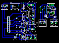
I did another board design, this time starting from the datasheet example. I took care to move capacitors away and tried to cram everything in a smaller space, but avoiding tracks under the small space between capacitor leads (leaving only tracks under resistors). I think the original board is something like 60x60mm, and I saved some 10mm in each direction... 😀
I am designing this board a bit as a sport also, because I am in vacations at my parent's home, and I left all my electronics stuff in my home. 🙂
I did another board design, this time starting from the datasheet example. I took care to move capacitors away and tried to cram everything in a smaller space, but avoiding tracks under the small space between capacitor leads (leaving only tracks under resistors). I think the original board is something like 60x60mm, and I saved some 10mm in each direction... 😀
Attachments
The third leg of the trimmer should also be connected. If the wiper looses contact (tear and wear), the resistance would be infinite. With alls pins connected, at least the resistance is limited to the value of the trimmer. Connect pin 3 to the LM and connect pins 1 and the wiper together. But check, if pins 1 and 3 are really the ends of the trimmer you buy. Sometimes those trimmers have the wiper on one of the outer pins instead of the center.
Bought components, and took of regulator
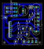
Hi. Today I bought the components, and now I'm sure of the size of the capacitors. So this is pretty much the last version of the board.
I decided to use first a very basic PSU, as the LM350 is in fact very expansive. So I just put the rectifier there with a 2200uF capacitor, and another small one near the chip because it brings luck. 🙂
How much voltage ripple should I allow? And how bad is it to leave all the power source circuit there at the same 60mm board? As for the rectifier bridge, it shouldn't heat much, right?
Perhaps I should think about some kind of Zener regulator?...
Attachments
ceramic capacitors for the low-pass filters
Another doubt: is there any reason I shouldn't use ceramic caps on these two RC filters that avoid the high-frequency ringing?
Another doubt: is there any reason I shouldn't use ceramic caps on these two RC filters that avoid the high-frequency ringing?
Re: ceramic capacitors for the low-pass filters
The best reason ever. 😀NIC1138 said:another small one near the chip because it brings luck. 🙂
Start with what you have. Anything that is as big as or bigger than what is shown in the datasheet is okay. Later you can try to add bigger capacitors and see, if you notice any changes.NIC1138 said:How much voltage ripple should I allow?
There are enough boards that work fine like that. It is good to maintain as much distance as possible to the signal traces. Small capacitors (100n) across the rectifier as snubbers help to suppress possible diode ringing.NIC1138 said:And how bad is it to leave all the power source circuit there at the same 60mm board?
Normally not much.NIC1138 said:As for the rectifier bridge, it shouldn't heat much, right?
Other than prejudice not. Avoid them in the signal path, if you can. But for snubber circuits, which is what the Boucherot cell basically is, ceramics are ideal.NIC1138 said:Another doubt: is there any reason I shouldn't use ceramic caps on these two RC filters that avoid the high-frequency ringing?
ripple man
I think I'll increase the rectifier capacitor. Right now, with 2200uF, the maximum ripple voltage would be approximately 1.5A/120Hz/2200uF = 5.6V, what looks quit large to me. I think I'll look at least for a 4700uF cap, if not larger.
Does anyone have information about the internal voltage reference this chip and similar ones have? And about how it tries to neutralize voltage source ripple? I noticed the voltage divider with a capacitor controlling some kind of current mirror. Does anyone imagine the value of these resistors?
The datasheet mentions in some point a test with a 0.5V ripple. I imagine it's not usual to have more than 1V ripple, so I'll try to get that low.
I think I'll increase the rectifier capacitor. Right now, with 2200uF, the maximum ripple voltage would be approximately 1.5A/120Hz/2200uF = 5.6V, what looks quit large to me.
I think I'll look at least for a 4700uF cap, if not larger.Does anyone have information about the internal voltage reference this chip and similar ones have? And about how it tries to neutralize voltage source ripple? I noticed the voltage divider with a capacitor controlling some kind of current mirror. Does anyone imagine the value of these resistors?
The datasheet mentions in some point a test with a 0.5V ripple. I imagine it's not usual to have more than 1V ripple, so I'll try to get that low.
The smaller capacitors will be sufficient regarding ripple. The datasheet shows only 100 µF. Don't even calculate the ripple for them. 
Your 5,6 V are peak. The effective ripple will therefore be ~4 V.
The 0,5 V you read are the conditions on which the ripple rejection was tested. The ripple rejection is given with 55 dB.
That means 4 V ripple on the rails will be reduced to 0,007 V ripple in the output signal. At the same time you have an output of 1,5 A, i. e. 12 V with an eight Ohm speaker, which means the ripple is ~65 dB below the signal. Even with the 100 µF capacitors the ripple would be nearly 50 dB below your signal, thus undetectable.
If you increase those capacitors, what you gain is performance in the lower frequency range.
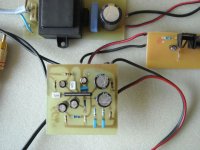
hello.
i built a headphone amp with a tda 2007a. voltage gain is a little bit reduced (r1....r4 are 1200ohm and 68 ohm).
the power supply is regulated by a lm317.
the foto shows first testing example with some spare parts that will be changed later on.
greetings.................
i built a headphone amp with a tda 2007a. voltage gain is a little bit reduced (r1....r4 are 1200ohm and 68 ohm).
the power supply is regulated by a lm317.
the foto shows first testing example with some spare parts that will be changed later on.
greetings.................
Attachments
- Status
- Not open for further replies.
- Home
- Amplifiers
- Chip Amps
- Building a TDA2007A 6+6W amplifier