Lately there were some discussions regarding improving the F2, with Nelson pointing out that 5x improvement was attained using some expensive devices. While there are hopes that such exotic devices can hit the market some time later, I continue to try to seek ways to use more readily and less expensive devices.
As previously noted, my primary aim is to look for devices which has a flat transconductance curve around the operating point. Looking at many MOSFETs I did not yet find a "good enough" candidate.
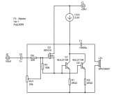
As F2 is essentially focused on Current drive, I started to think about current driving devices - BJTs. There are some BJTs showing a nice flat hfe curve, and I picked up MJL21194 as an example.
From the datasheet, we can see that the MJL21194 showed a pretty flat hfe from 0.5A to 2A. I developed the attached circuit topology and invite comments.
Here is a short description of this circuit:
I picked 2.5A total bias, like the FirstWatt F2. With a +/-1A swing, we get about 5W into 8 Ohm load. The current source can be exactly the current F2 one.
But this will drive the collector current to swing between 1.5A to 3.5A if we use only 1 MJL21194, not exactly the flattest portion of the hfe. So I put 2 in parallel. Each MJL21194 will be biased to 1.25A with a swing of +/- 0.5A (or from 0.75A to 1.75A). This lies neatly on the flattest hfe zone.
Being a current driven device, we need to put a MOSFET IRF610 in front to work as the voltage to current conversion device. The hfe is assumed to be about 80, so the base current will be 15mA, and the swing is +/- 6mA. Having 2 MJL21194, the IRF610 should be biased at 30mA and swing +/12mA. This is small signal level variations so the gm of the IRF610 can be assumed to be constant.
Combining a flat hfe and a constant gm, I believe we should be having a rather linear system here?
The other resistors set up the bias. R3 helps the MOSFET to self-biased, establishing the Vgs. Pot RV1 should set the collector voltage to 1/2 of the Vcc (I am not 100% sure if this will work)...Some more considerations are needed to adjust system gain etc..
Would like to take comments on this topology.
As previously noted, my primary aim is to look for devices which has a flat transconductance curve around the operating point. Looking at many MOSFETs I did not yet find a "good enough" candidate.
As F2 is essentially focused on Current drive, I started to think about current driving devices - BJTs. There are some BJTs showing a nice flat hfe curve, and I picked up MJL21194 as an example.
From the datasheet, we can see that the MJL21194 showed a pretty flat hfe from 0.5A to 2A. I developed the attached circuit topology and invite comments.
Here is a short description of this circuit:
I picked 2.5A total bias, like the FirstWatt F2. With a +/-1A swing, we get about 5W into 8 Ohm load. The current source can be exactly the current F2 one.
But this will drive the collector current to swing between 1.5A to 3.5A if we use only 1 MJL21194, not exactly the flattest portion of the hfe. So I put 2 in parallel. Each MJL21194 will be biased to 1.25A with a swing of +/- 0.5A (or from 0.75A to 1.75A). This lies neatly on the flattest hfe zone.
Being a current driven device, we need to put a MOSFET IRF610 in front to work as the voltage to current conversion device. The hfe is assumed to be about 80, so the base current will be 15mA, and the swing is +/- 6mA. Having 2 MJL21194, the IRF610 should be biased at 30mA and swing +/12mA. This is small signal level variations so the gm of the IRF610 can be assumed to be constant.
Combining a flat hfe and a constant gm, I believe we should be having a rather linear system here?
The other resistors set up the bias. R3 helps the MOSFET to self-biased, establishing the Vgs. Pot RV1 should set the collector voltage to 1/2 of the Vcc (I am not 100% sure if this will work)...Some more considerations are needed to adjust system gain etc..
Would like to take comments on this topology.
Attachments
Last edited:
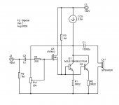
Looking more and more into the concept, mistakes are found. Also, how the system will behave when power-on is still not sure -- will the circuit survive through the power-on and settle on the bias points, or it will latch up somewhere?
A correction made:
The resistor linking the Gate/Source of IRF610 was a mistake. MOSFET cannot be "self-biased" this way. Even for JFET, the position of the resistor was not correct.
How the MJL21194 turns on during power-up? I put a high impedance path of 1M resistor to Vcc, hoping to pull it up during power-on to kind-of crank up the Vbe and so turn-on the transistor. When it turns on, it will demand base current and hopefully draw it through IRF610 and also turn it on.
Any mistakes or comments, from anyone?
Attachments
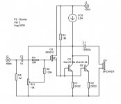
Take a look at how Nelson biased the gate voltage of the IRFP240 in the F2, copy that for your 610. There's no reason for a 610 front end to have lower input impedance than a stock F2.
R3 should tie the 610 source to ground, using a much lower value, to get some decent current through the 610.
R3 should tie the 610 source to ground, using a much lower value, to get some decent current through the 610.
Thanks, yes I missed the 100k connecting the gate to the pot wiper. Now added, and also tune down the pot value to 10k, looking more like the stock F2.
But I am not that sure about your comment on R3 and need to digest it more. My concept was to ensure that the IRF610 convert voltage-variations from the input into current-variations of the Base of MJL21194s. With a low impedance R3 shunting the Source to GND, how will this affect the Base current variations is not clear to me. I am not sure if there is a linear relationship here anymore. Maybe the best way is to do experiement?
But I am not that sure about your comment on R3 and need to digest it more. My concept was to ensure that the IRF610 convert voltage-variations from the input into current-variations of the Base of MJL21194s. With a low impedance R3 shunting the Source to GND, how will this affect the Base current variations is not clear to me. I am not sure if there is a linear relationship here anymore. Maybe the best way is to do experiement?
Attachments
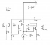
Might have found a solution to the IRF610 bias question. Removing the R3 1M resistor, I hook up the Source to GND with a 10mA current source.
The presence of this CCS should help the IRF610 to conduct during power-on, and eventually settle down to the desired bias current. Now this will become 30mA thru Base of MJL21194 + 10mA thru CCS = total 40mA.
While the current variation in the IRF610 as a result of the transconductance will all pass to the Base of the transistor, fulfilling the intended task.
Nevertheless, the circuit is getting a bit more complicated than I would prefer.
Attachments
- Status
- Not open for further replies.