The circuit on attached is a contour (variable loudness) circuit of Nakamichi 410 preamplifier. I’m wondering that why they used two sets of 22uf capacitors and 100kOhms resistors; C501, R501 and C503, R503. Are these components be buffer circuits? And why didn’t they place them after the switch to reduce the components, using only one set of R and C instead of using two for IN and OUT switch position?
Attachments
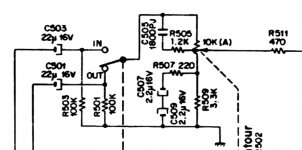
The switch changes the input of the volume pot and bypass the previous stage.
The capacitors block DC from the inputs and the 100k resistors discharge the caps to prevent a "crack" when switching.
A Buffer is an active circuit and needs at least one transistor or opamp. It doesn't amplify the voltage but has a high input and low output impedance
The capacitors block DC from the inputs and the 100k resistors discharge the caps to prevent a "crack" when switching.
A Buffer is an active circuit and needs at least one transistor or opamp. It doesn't amplify the voltage but has a high input and low output impedance
The switch changes the input of the volume pot and bypass the previous stage.
The capacitors block DC from the inputs and the 100k resistors discharge the caps to prevent a "crack" when switching.
If I remove the switch from the circuit assuming there's no bypass path, can I eliminate the 100k resistors?
And, do I need to leave the capacitors at the same place?
Last edited:
Perhaps there were shifts in the DC voltage level in the original circuit. When switching clicks. It is also a high-pass filter along with a potentiometer.
You can measure the voltage acoss the cap with a voltmeter. When it is <+/- 10mV you can try to take out the C and R. Or you leave both C and R.
Just looked again at the schematic and you can remove the 100k and leave the C if you have removed the switch. the pot is 100k to gnd.
Just looked again at the schematic and you can remove the 100k and leave the C if you have removed the switch. the pot is 100k to gnd.
Thanks very much. I found another circuit in its brother, Nakamichi 630, which has the same configuration as the 410's but without bypass switch. It was eliminated R but remained C as you mentioned.
May I ask one more question? What is the responsibility of R511 (470 Ohms)? It appears in both 410 and 630. How important is it?
- Home
- Source & Line
- Analog Line Level
- Buffer circuits, aren’t they?