Hi!
I have been following the ClassD-forum for a while but I haven't seen any real info on this topic.
If you take two self-osc-amps and connect them as a bridge then there is no synchronization between the two amp's. There should be a fair chance of getting a lot of noise at the output as a result of inter-modulation.
If the two half's of the bridge is controlled from the same modulator then they would be in sync. But then there's a problem with the feedback as it is pretty complicated to take the feedback from the analog output. Taking the feedback's before the LPF would be easier, but those are out of phase. I can't figure out how this is to be fed back to the modulator?
I've tried to make a bridge that's in sync and with feedback taken before one of the LPF. This works fine but one half of the bridge is running without feedback and this should/could cause a lot of problems.
Does this make any sense? Any inputs/comments are of cause welcome.
Hi,
here is link to the US patent application 20050068121. I think you will find some ideas in there.
Basically, bridged synchronised modules only need good coupling at the switching frequency. With UcD this can be achieved by placing capacitor across the load and also has added benefit of almost eliminating output HF ripple. For feedback before output filter look at provided link. With one modulator you only need to apply fully differential feedback.
Best regards,
Jaka Racman
Thanks for you reply.
I must admit that I don't get it... if I bridge two half-bridges and connect a capacitor across the load the to outputs will be in sync and I only need feedback from one of them?
Jaka: "With one modulator you only need to apply fully differential feedback." Is that a diff feedback before or after the LPF? Before the filter the signal is a fast square wave and I cant See how a diff-amp could be fast enough to process this signal.
After the filters the signal is mostly a sine wave and the a "normal" diff-amp would do the job. I get that part, but then there's the problem with the phase-shift in the filter. Please comment.
I'm trying to simulate the freq-response of the amp with a feedback path after the LPF but that's a real pain in PSpice. Wouldn't it give the same result if a take an ideal op-amp and ad a LPF instead of the Self-Osc-ClassD-amp?
Regards
TroelsM
EDIT: Forgot one thing: I can't see the pics/drawings in the patent-link.. Any ideas?
Hi,
first how to view images .
Cap across load works only with two UcD modules each having it's own modulator. That works because their feedback is taken after the filter.
With one modulator things are no different in full bridge than in half bridge. If you take feedback before output filter you need integrator for the modulator. Just use differential integrator instead of a single sided one.
You are right about the model, but results are accurate up to the one half of the switching frequency (in clocked designs).
A little more accurate model is presented below. It takes bidirectional power flow into account, so it also models power supply pumping in half bridge.
*
* Snchronous Buck power stage operating in continious mode.
* Based on Generalized Switched Inductor Model from
* Sam Ben-Yaakov presented on APEC03.
* Translated to LTSpice.
* Includes duty cycle limiting from 1% to 99%
*
.subckt YaakovSynchronousBuck Vin+ Vin- a gnd Din
Rinductor 2 1 {Rinductor}
Lmain gnd 2 {Lmain}
RswU b Vin+ {Rsw}
B§EDoff Doff gnd V=table((1-V(Don)),0.01,0.01,0.99,0.99)
B§Ga gnd a I=I(Lmain)
B§EL 1 gnd V=(V(a,b)*V(Don)+V(a,c)*V(Doff))
B§Gb b gnd I=I(Lmain)*V(Don)
B§Gc c gnd I=I(Lmain)*V(Doff)
RDin Din gnd 1Meg
B§EDon Don gnd V=table(V(Din),0.01,0.01,0.99,0.99)
RswL c Vin- {Rsw}
.param Lmain = 100uH
.param Rinductor = 100m
.param Rsw = 100m
.ends YaakovSynchronousBuck
More about the model can be seen here.
Best regards,
Jaka Racman
TroelsM said:
If the two half's of the bridge is controlled from the same modulator then they would be in sync. But then there's a problem with the feedback as it is pretty complicated to take the feedback from the analog output.
Wait till Nelson invents self-oscilating class D super symetry.
😀
ehh..?
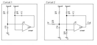
I'm sorry but I don't get it. Please see the attached picture.
Circuit 1 is a standard diff. int. but it cannot be used here without some modification. Curcuit 2 is my first idea, but I cant figure out if this is the right way to go?
The "OutputA" and "OutputB" are the feedback's from each side of the bridge before the LPF's.
If anyone could recommend literature about this topic I would be glad.
Regards
TroelsM
EDIT: I can't see the pic.. only a red cross? Can you see it?
Re: Re: Bridge with two self-osc ClassD amps?
Just Hypex's full bridge ucd idea in technical information on their site?
differential in / differential out power comparator + differential NFB
Just Hypex's full bridge ucd idea in technical information on their site?
differential in / differential out power comparator + differential NFB
darkfenriz said:
Wait till Nelson invents self-oscilating class D super symetry.
😀
Re: Re: Re: Bridge with two self-osc ClassD amps?
Exactly. They don't sell such a beast though, but there's enough info on here that you can possible make your own. I made a few sims to that effect. However the half bridge is just as good.
If you wait for others to do for you you'll be waiting a long time, and honestly I don't find IcePower all that impressive, could we for instance expect super symetrical smoking zobel's? Nah thank you.
KM has done excellent work as a scholar, his papers are excellent, but I think IcePower could well be refined, and there hasnt' been anything new from him in awhile, so don't hold your breath.
I think it far more productive to give someone who's interested a little push and a tip here and there, they're likely to produce something long before some commercial fat cat, and even be willing to share with those who've helped them get there, whereas with the commercial fat cat's we're lucky if we can even steal it off a shelf.
Kenshin said:Just Hypex's full bridge ucd idea in technical information on their site?
differential in / differential out power comparator + differential NFB
Exactly. They don't sell such a beast though, but there's enough info on here that you can possible make your own. I made a few sims to that effect. However the half bridge is just as good.
If you wait for others to do for you you'll be waiting a long time, and honestly I don't find IcePower all that impressive, could we for instance expect super symetrical smoking zobel's? Nah thank you.
KM has done excellent work as a scholar, his papers are excellent, but I think IcePower could well be refined, and there hasnt' been anything new from him in awhile, so don't hold your breath.
I think it far more productive to give someone who's interested a little push and a tip here and there, they're likely to produce something long before some commercial fat cat, and even be willing to share with those who've helped them get there, whereas with the commercial fat cat's we're lucky if we can even steal it off a shelf.
Is it possible to implement this BridgeUCD with the modulator (first triangle) only +/-5V fast comparator, while the input is only (+), (-) input is grounded? The grounded (-) input and the output feedback resistor will make a voltage divider that push the comparator more than +/-5V?
Attachments
Then you will get the input voltage as a common-mode component on the output. You should drive this arrangement from two complementary ground-centered signals instead. The voltage requirements on comparator inputs will depend on the amount of carrier residuals involved.
Hi, EVA,
I'm not clear. Is it possible to use +/-5V for the first triangle, while the rails are +/-40V? That first triangle has no ground reference, where should the ground reference be?
I'm not clear. Is it possible to use +/-5V for the first triangle, while the rails are +/-40V? That first triangle has no ground reference, where should the ground reference be?
It might be questionable whether it is necessary at all to synchronise two self-oscillating amps that are running in bridge-mode.
Regards
Charles
Regards
Charles
You need a ground reference, preferably at the same RF potential as the ground planes, the case and the input and output wiring (otherwise you will have trouble as I had).
If by "triangle" you mean the comparator, you can use a +/-5V part if you adjust component values so that the carrier residual plus the input signal does not exceed +/-5V at the inputs.
The other part of your question is related to full bridge centering and differential inputs and is a bit harder to reply. Try imagining that the amplifier is linear and use your brain and op-amp theory a bit. In the circuit that you posted the common-mode input voltage becomes actually the center reference voltage for the outputs, and the differential input voltage becomes the output amplitude with respect to the center. If you want to reference the comparator to any other voltage, you have to provide a common-mode reference for output centering and ensure that the input voltage has no common-mode component...
BTW: You don't need to synchronize self-oscillating amplifiers, crosstalk does not follow the rules of clocked modulators, in my experience it appears as an increased noise floor when playing loud.
Hi, Phase_Accurate, EVA,
I should say making a "full bridge UCD" instead of "bridging 2 unit of UCD" 😀
The comparator I intend to use is LM360. They have complementary output, so I tought, why don't use both the outputs for full bridge UCD. This is where it started.
The first problem is this device is only +/-5V. With a normal (half bridge) UCD, this is not a problem at all, if we make inverting UCD, we ground the +input, so no problem using +/-5V device here. The -input will cannot go far from 0V.
But will full bridge like that, there's no insurance that +/-5V will be enough, because (+) and (-) input voltages cannot be predicted. (as long as it is assured that (+) and (-) input voltages always the same magnitude+180deg difference, there's no problem)
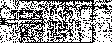
From UCDBP.pdf, I got that picture above. It's a theoritical diagram about how to make full bridge UCD with 1 main comparator.
This scheme is very interesting for me. It's similiar to SuSy, where any one sided disturbance will be disappear from loudspeaker's POV. It's different than bridging 2 modules.
I don't know how far more difficult this will be, than making half bridge UCD. Hypex don't make one commercial out of this is one clue (I assume the 400 or 700W version could be made with this scheme, yet they force to use mosfet >100V instead).
I should say making a "full bridge UCD" instead of "bridging 2 unit of UCD" 😀
The comparator I intend to use is LM360. They have complementary output, so I tought, why don't use both the outputs for full bridge UCD. This is where it started.
The first problem is this device is only +/-5V. With a normal (half bridge) UCD, this is not a problem at all, if we make inverting UCD, we ground the +input, so no problem using +/-5V device here. The -input will cannot go far from 0V.
But will full bridge like that, there's no insurance that +/-5V will be enough, because (+) and (-) input voltages cannot be predicted. (as long as it is assured that (+) and (-) input voltages always the same magnitude+180deg difference, there's no problem)
From UCDBP.pdf, I got that picture above. It's a theoritical diagram about how to make full bridge UCD with 1 main comparator.
This scheme is very interesting for me. It's similiar to SuSy, where any one sided disturbance will be disappear from loudspeaker's POV. It's different than bridging 2 modules.
I don't know how far more difficult this will be, than making half bridge UCD. Hypex don't make one commercial out of this is one clue (I assume the 400 or 700W version could be made with this scheme, yet they force to use mosfet >100V instead).
This is not a balanced input, it needs symmetrical input voltages to produce a centered output. However , you don't seem to understand that even when the input and ouput signals cancel the common-mode input voltage to the comparator, as in inverting arrangements, you still have to deal with carrier residual which has some amplitude too (the more the better noise margin). See the oscilloscope capture that I published in the other thread.
Isn't the differential voltages between (+) and (-) inputs are supposed tobe very little?However , you don't seem to understand that even when the input and ouput signals cancel the common-mode input voltage to the comparator, as in inverting arrangements, you still have to deal with carrier residual which has some amplitude too
How can you control that with IC (8 pin comparator)?(the more the better noise margin)
lumanauw said:
Isn't the differential voltages between (+) and (-) inputs are supposed tobe very little?
How can you control that with IC (8 pin comparator)?
No, the AC voltage between comparator inputs is a fraction of the carrier residual that appears at the output, 50% or so. This is what causes it to oscillate and work as a modulator.
Lumanauw.
A full-bridge amp based on the ucd topology is fairly straightforward.
I have designed a low-power (60W) full-bridge ucd-based amplifier for my employer to go into a voice-alarm amplifier unit to feed an output step-up transformer to drive 100V ceiling speakers. This design had to run on unipolar power rails. (I had supplies of +5V, +12V and +42V available)
Although as a commercial design I cannot publish a circuit diagram, the prototype used a two-transistor (+ current source) differential amplifier, a TL712 as the high-speed differential output comparator, two LM5106 gate drivers, and four D-PAK NXP mosfets for the output bridge.
(The use of the NXP mosfets was to ensure that we comply with the Philips requirements for licence-free use of the UCD patent).
The use of a ground-referenced TL712 comparator (powered by +5V) for the modulator required the two-transistor diff amp as the input, so that I could ac couple the input signals and have the diff-amp self bias at 21V (half the main output bridge supply voltage).
Driving an outout transformer meant that I had to have a very low output offset voltage (less than 10mV) to prevent excessive dc current flowing in the low-resistance primary of the output transformer.
The design works very well, but to save costs, I will replace the TL712 and combine the input diff-amp with a 'Bruno Putzeys' style discrete component comparator for the production version. This will keep Philips/NXP happy as the discrete semiconductors will also be NXP parts.
By the way, when I was dealing with Philips/NXP to ascertain the requirements for licence-free use of the UCD topology, it certainly seemed that they had lost interest in this excellent design technique that they hold the patent rights to. I was surprised by this!
- Status
- Not open for further replies.
- Home
- Amplifiers
- Class D
- Bridge with two self-osc ClassD amps?