Looking at your photo of the nice clean internals, you may have to disassemble to get access to bias and offset adjust trimpots, can't see these on the FE board in your photo. Definitely worthwhile in measuring power supply +/- DC voltage under load with a scope as well as measuring those DC voltages with a DMM to compare to design schematic - plenty of those around for this amp.
Good luck with the fix however you proceed with it - one thing is for sure, these beauties are worth every cent in restoring to 100% condition.
Have you had a go at measuring the bias (volts across emitter resistors) and the DC offset voltage. Measuring the bias volts across each emitter resistor will lead you to any output transistor problems. Also, you mentioned the difference in emitter resistance values - not sure, but maybe way back then the resistors might have been 10% tolerance, replacing with more modern close tolerance and better resistors will help. More than likely the caps will be OK, I bet NP would say they will be fine.
I'll get to measuring the bias soon.
The emitter resistors are 5% tolerance.
I was able to quickly measure the DC offset and it was 54mV and continued to creep upward with the unit powered on. If there's a 2N5566 JFET in there, it's coming out, but I've seen many different schematics floating around so I'm not sure which one is applicable to this unit yet.
For reference, I have a Hadley 622 from the mid-60s that uses a dual NPN for the differential pair. Once I swapped the original unit out for a high-β matched MAT-12 dual NPN, and centered the pot where I got a reading that floated around 0mV. At that point I just took the pot out and used two resistors in its place. At that point, the DC offset was +2mV and -2mV and stable as measured on both channels. Power on and off is completely silent.
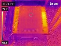
For this particular unit, I'm beginning to think the adhesion of the heatsinks to the plate the output transistors are all mounted to is the issue. Keep in mind that each side of the heatsink actually is four pieces and see the photos below:
By my own logic, if there was an issue with any single transistor, we'd likely see a difference in heat with the associated 1 Ω emitter resistor. I took these photos quickly upon power on before the heat had the chance to spread out and it clearly looks limited to the middle two heatsink segments while the board itself appears acceptably even.

I decided to practice disassembly on my S/300. That unit required exactly zero use of the soldering iron and was not at all challenging to disassemble. The SA/1 will be the same with heavier chunks and maybe a few additional wires to the meter (that I may need to unsolder). So, I'll ask, what special expertise is required here? Why do I need drive 12+ hours dropping off and picking up amplifiers? I'll answer: there is nothing here that requires the drive or special expertise, there just isn't. I could replace every part on this board on a Saturday morning (obviously won't given someone already had a little fun with the resistors). The reality is that these techs, including the protectionists scattered around this forum aren't going to be around forever and unless some people take some initiative and start learning how to fix this gear and sharing their experiences doing so, there won't be much of a community in about 10-15 years. Maybe that doesn't matter to most of you, but at 31, it matters to me.


Post 13 photo shows the reason for the uneven heat distribution which is probably slight , which is the gaps from transistor bar from front and rear. Likely the amp is fine.
Post 13 has no photo.Post 13 photo shows
https://www.diyaudio.com/community/...shold-sa-1-pair-from-1988.385741/post-7010878
Unless this newfangled forum database is showing different numbers to different readers?
I think you will find that Nelson was referring to the response in post #13 when viewing the photo in post #7.
It's not the gaps in the heatsink (though those should be fixed), it's the lack/poor quality of the thermal paste between the heatsink and the t-bar the transistors are mounted to. Here is what the S/300 looked like between the heatsink and the t-bar. The heat across this unit's heatsinks was also uneven. Additionally, the gaps between the segments are due to sloppy assembly as there's plenty of clearance to make sure those heatsinks are contacting each other. I'll add thermal paste between the segments as well as there was none. If the T-bar is hotter than the heatsinks, which it certainly would be with little contact as seen here, that is a problem.

Work continues... almost done with a legible schematic, free from errors for all. It even lights up.

I think it's not an LED, it's an optocoupler. There's a LED and a photo transistor inside but light is not visible from the outside world.
Posted this earlier, but had to correct a couple of errors/omissions I found after I posted. This was a lot of work, but had to be done given I couldn't find the correct schematic for early Optical Bias units made before 1989. Haven't pulled the boards from the NOS amps (Series I), but beyond the type of resistors, the layout looks nearly identical from what I can tell. However, I will create another version with any values updated. Please let me know if you see any issues, I don't want another schematic floating around that has errors wasting someone's time.

I have one of the SA-1s back together.
What was done:
-Completely disassembled heatsinks and removed all transistors to clean and apply new thermal paste. Replaced numerous mica insulators. It took ~50 grams of paste to do the job.
-Replaced all four filter capacitors.
-Replaced all emitter resistors.
-Replaced tantalum capacitor and 10uf polyester cap on driver board with polypropylene units. The 10uf fit fine.
-Replaced the 2N5566 with a IFN5564.

The old thermal paste needs to be replaced if you have one of these amplifiers. On my unused unit, much of it had run down the side of the heatsinks and pooled near the bottom of the chassis. I found numerous areas that had essentially no coverage. This means that your heatsinks won't properly warm up and as a result your bank of transistors could be too hot. Yes, there is certainly a margin for error here, but given the cost of these amplifiers, I don't want my heatsinks at different temperatures and I wouldn't have in 1989 if I had bought them then. The second picture is how it does and should look.
The amplifier sounds good, but I will A/B against the still original unit and report back my findings. Power consumption after service is much lower but I will likely need to set the bias. Certainly a good sign though that the unit isn't consuming 500+ watts at power on. I'll also measure the DC at the outputs.
Before:
.jpg")
After:


What was done:
-Completely disassembled heatsinks and removed all transistors to clean and apply new thermal paste. Replaced numerous mica insulators. It took ~50 grams of paste to do the job.
-Replaced all four filter capacitors.
-Replaced all emitter resistors.
-Replaced tantalum capacitor and 10uf polyester cap on driver board with polypropylene units. The 10uf fit fine.
-Replaced the 2N5566 with a IFN5564.
The old thermal paste needs to be replaced if you have one of these amplifiers. On my unused unit, much of it had run down the side of the heatsinks and pooled near the bottom of the chassis. I found numerous areas that had essentially no coverage. This means that your heatsinks won't properly warm up and as a result your bank of transistors could be too hot. Yes, there is certainly a margin for error here, but given the cost of these amplifiers, I don't want my heatsinks at different temperatures and I wouldn't have in 1989 if I had bought them then. The second picture is how it does and should look.
The amplifier sounds good, but I will A/B against the still original unit and report back my findings. Power consumption after service is much lower but I will likely need to set the bias. Certainly a good sign though that the unit isn't consuming 500+ watts at power on. I'll also measure the DC at the outputs.
Before:
After:
Attachments
Last edited:
Both amplifiers are finished. Across both, I replaced 80 emitter resistors, 8 filter caps, and a few other capacitors along with the 2N5566s (to IFN5564s). I will get back to these at some point later this year and replace the remaining components on both boards.

The improvement in sound was noticeable, but I believe the more important accomplishment is that the amps should be more reliable. Before replacing the eight filter caps, both units consumed over 500 watts when powered on. After replacing these very large, expensive caps, the units never exceeded 330 watts. The originals are clearly leaky and while this may have improved over time, it's a big difference. The improvement in thermal performance by disassembling and applying real thermal paste has already been shown above and was consistent across both amplifiers. I want to note that the application of the original thermal paste-like material was inconsistent and in fact I found multiple unrelated issues on these brand new amps that should've been caught by QC nearly 35 years ago. After about an hour of use, the amplifiers got up to ~115 degrees or in the ballpark for bias spec. At that point, power consumption had dropped from the 330 watts at power on.
Second amp after 20 mins:

First amp after 20 mins:

One amplifier has ~35mV at the outputs and the other around ~60mV. This did not improve noticeably with anything that I did and while I understand this will not affect the speakers or performance of the amps, I find it ...interesting that there's no way to adjust this when the amp isn't inherently completely balanced. There is also still a thud at power on which means it's almost certainly the switch, that of course can't be sourced from what I can tell.
In terms of sound, they're nice, but I can't say I'm completely satisfied. The bass is of course incredible, but the highs aren't as amazing as advertised. There is a vagueness and a bit of harshness the higher up one goes in the frequency spectrum and I would hands-down take my Hadley 622C over these even with its less authoritative low frequency performance and limitations in terms of speakers it can be used with. Sorry to say it's not a subtle difference, either. The Hadley also doesn't send a thud through my speakers or have a DC offset of more than +/- 2mV.
Beyond that, these are well-built, well-designed amplifiers. They come apart easily if you know the order to do things and they go back together relatively easy as well. These are not complicated compared to other amps I've worked on. The boards are great quality (even though they should've had markings) and the quality of the anodizing and the aluminum is excellent.
The metal foil resistors on my S/300 II boards seem to be a big improvement and I hope these components take these amps a notch or two higher.
The improvement in sound was noticeable, but I believe the more important accomplishment is that the amps should be more reliable. Before replacing the eight filter caps, both units consumed over 500 watts when powered on. After replacing these very large, expensive caps, the units never exceeded 330 watts. The originals are clearly leaky and while this may have improved over time, it's a big difference. The improvement in thermal performance by disassembling and applying real thermal paste has already been shown above and was consistent across both amplifiers. I want to note that the application of the original thermal paste-like material was inconsistent and in fact I found multiple unrelated issues on these brand new amps that should've been caught by QC nearly 35 years ago. After about an hour of use, the amplifiers got up to ~115 degrees or in the ballpark for bias spec. At that point, power consumption had dropped from the 330 watts at power on.
Second amp after 20 mins:
First amp after 20 mins:
One amplifier has ~35mV at the outputs and the other around ~60mV. This did not improve noticeably with anything that I did and while I understand this will not affect the speakers or performance of the amps, I find it ...interesting that there's no way to adjust this when the amp isn't inherently completely balanced. There is also still a thud at power on which means it's almost certainly the switch, that of course can't be sourced from what I can tell.
In terms of sound, they're nice, but I can't say I'm completely satisfied. The bass is of course incredible, but the highs aren't as amazing as advertised. There is a vagueness and a bit of harshness the higher up one goes in the frequency spectrum and I would hands-down take my Hadley 622C over these even with its less authoritative low frequency performance and limitations in terms of speakers it can be used with. Sorry to say it's not a subtle difference, either. The Hadley also doesn't send a thud through my speakers or have a DC offset of more than +/- 2mV.
Beyond that, these are well-built, well-designed amplifiers. They come apart easily if you know the order to do things and they go back together relatively easy as well. These are not complicated compared to other amps I've worked on. The boards are great quality (even though they should've had markings) and the quality of the anodizing and the aluminum is excellent.
The metal foil resistors on my S/300 II boards seem to be a big improvement and I hope these components take these amps a notch or two higher.
Last edited:
Well, you have done a very good rebuild job there, the amps even look brand new. I hope you enjoy them for many years to come. Certainly worth every cent you spent on them.
This is due to the non-symmetry of the input JFET transistors.One amplifier has ~35mV at the outputs and the other around ~60mV. This did not improve noticeably with anything that I did and while I understand this will not affect the speakers or performance of the amps, I find it ...interesting that there's no way to adjust this when the amp isn't inherently completely balanced. There is also still a thud at power on which means it's almost certainly the switch, that of course can't be sourced from what I can tell.
To adjust the minimum output voltage value, you will need to make changes to the operating points of the input diff stage.
this is as it should be, because Miller frequency correction is applied.In terms of sound, they're nice, but I can't say I'm completely satisfied. The bass is of course incredible, but the highs aren't as amazing as advertised. There is a vagueness and a bit of harshness the higher up one goes in the frequency spectrum and I would hands-down take my Hadley 622C over these even with its less authoritative low frequency performance and limitations in terms of speakers it can be used with. Sorry to say it's not a subtle difference, either.
P.S. You have done a lot of work on setting up this device - it's very cool ...
This is due to the non-symmetry of the input JFET transistors.
To adjust the minimum output voltage value, you will need to make changes to the operating points of the input diff stage.
this is as it should be, because Miller frequency correction is applied.
P.S. You have done a lot of work on setting up this device - it's very cool ...
Thanks very much.
Both amps had similar DC offset readings before and after the JFET replacement so I'm guessing a resistor is out of spec or transistors are poorly matched on the driver board. The JFETs themselves are closely matched enough to have potentially very low DC offset in the proper circuit. From the batch I sampled, the power transistors appeared not to be β matched so it would stand to reason the rest of the transistors weren't either. As I mentioned in another thread, just because a circuit is β insensitive doesn't mean that β doesn't matter at all. But, I suppose it's more likely one of the critical resistors has simply drifted.
Last edited:
Posted this earlier, but had to correct a couple of errors/omissions I found after I posted. This was a lot of work, but had to be done given I couldn't find the correct schematic for early Optical Bias units made before 1989. Haven't pulled the boards from the NOS amps (Series I), but beyond the type of resistors, the layout looks nearly identical from what I can tell. However, I will create another version with any values updated. Please let me know if you see any issues, I don't want another schematic floating around that has errors wasting someone's time.
View attachment 1051232
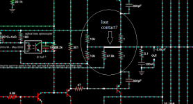
maybe contact is lost? see Attachment.
because it turns out that the output stage of Shiklai was left without NFB.
Attachments
Hadley, you perfectly illustrate the proverb "Value does not wait for the number of years"
You have done a remarkable job with patience and mastery, my respect.
You have done a remarkable job with patience and mastery, my respect.
- Home
- Amplifiers
- Solid State
- Brand New Threshold SA-1 Pair from 1988