Hello,
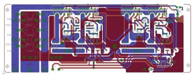
I recently designed a PCB for the BPA 200, following the schematic recomended by NS in AN1192. As I am quite a noob in PCB design I would like to hear a few opinions regarding the layout of this PCB. I would ultimately like to build this amp and so would appreciate any advice that can save me some trouble in the long run.
I haven't created a sketch file in eagle for this board, went directly to PCB, but there should not be any mistakes in the wiring (hopefully).
A few words about the PCB.
The power traces are going to be thickened by soldering a 2 mm diameter wire onto them, when the amp is built.
I tried to shield the signal paths with ground planes, also tried to have a mixed ground plane-star ground design.
Thank you!
Attachments
I was a bit asleep when i wrote the above post... i meant to say schematic file in eagle.
Also forgot to mention that as the input buffer for the board im going to use opa211, not the LF411, as i have a few opa211 and beacuse a smd version better fits the curret PCB layout. The servos are LF411cn, as I think the recomended NS schematic is designed with those in mind.
Would greatly appreciate any advice regarding the components used and the PCB layout.
Thank you!
Hi,
do you know why you are fitting an input buffer?
Do you know what the brief for the input buffer should be?
Can you define the specification for that input buffer?
Could any of these specifications be better achieved another way, eg. locating the buffer as a driver at the output of the source?
Once you have these answers, then you can start designing your buffer and only then can you determine which opamp might be suitable. You seem to have all this back to front!
I could ask a similar series of questions about the proposed Ground Plane.
Hello,
The answers to the first and third questions I found in AN1192.
I do not want to put the buffer on the output of the source because i would like the amplifier to work with a multitude of sources, I could put it on a separate board inside the amp thou, but i prefer having as little boards and cables as possible.
I searched for other op-amps but the opa211 seemed to offer the best performance, but after reading its data-sheet again I saw that it has good performance with low source impedances, so opted instead for the opa827. I think this one is more appropriate as it has a jfet input and is recommended for high source impedances. Did I get it right this time?
What did you want to say about the ground plane?
I asked thees questions because nothing can beat experience in designing a proper circuit, and I know I do not have this experience, but am willing to learn, I just need a few directions on where to start.
Thank you for your time Andrew T !
- Status
- Not open for further replies.