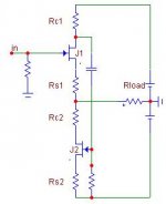
push Pull condition
to those interested
The value to be assigned to the upper collector resistor of a WF to
obtain Push-Pull operation is, as a first approximation , given by:
RC1= RS2 +(RC2+ri2+RS2+2*Rload)/m2
where ri2 and m2 are the internal resistance and the
gain of the lower tube, respectively.
The results derive from a linear analysis. Gate currents neglected,
lower gate resistance neglected.
To my surprise, Rc1 for PP depends only on the lower part of the circuit.
So for both the boberly WF of post #2 and the WF proposed in post #52 we have, if the load resistance is small:
RC1=RS2+ Ri2/m2
regards
Federico
Attachments
When push pull comes to shove.
You guys are completely missing the point I believe. The drain resistor for the upper jfet follower determines the amount of current gain in the circuit. The drain resistor multiplied the transconductance (or Gm plus 1/Rsource if using a source resistor for the bottom jfet) of the lower jfet determines the current gain of the circuit. As such the current variations through the top fet follower are about 1/10 of the current delived to the load. This is about 20dB of negative feedback. Reducing the amount of feedback will usually increase the distortion for a circuit. making the drain resistor too large will cause issues with stability as well as modulation of the drain to gate capacitance of the upper jfet follower.
BTW... This circuits power supply rejection could be greatly increased by making the current buffer a P channel jfet between the positive supply and the output. Any guesses why? The Ids of the current source to the negative rail will have to be the sum of the Ids of the two jfets connected to the postive supply. With a couple of device changes the circuit could be made DC coupled with even greater negative feedback. HINT: Go reread Mr. Pass's article on DIY op amps on his website.
PS No help from the experts until we have a few guesses. This means you; Nelson, John, Jocko, and Jam!
I breadboarded the simple follower with 2SK389s and two source resistors of 10 ohms. The output offset was 6mV. I thought it would have been lower? I have other 2SK389s and will plug them in and see what I get. Then I'll do some adjusting on the source resistors.
I did some more substitutions and the output offset of the 2SK389's were from 4 to 7mV. I also tried some 2SK170's which resulted in lower output offset if you substituted until you got a good match. Out of 10 2SK170's there was only one FET that didn't result in a output offset of less than 7mV and the best match being 1mV. The one thing that I did notice was the 389's didn't drift at all while the 170's showed some drift, but the amount was only fractions of millivolts. It just shows that the thermal tracking is better with the dual package. If you coupled them together like Fred showed then they would track much better, but I don't see it as an issue, just that little extra.
The frequency response was better than the generator I have to test with, in the MHz.
I suppose the next step is to put on some connectors and a pot. and have a listen!!
BDP
Hi Fred, All,
I do not understand some of your sentences. Maybe a problem of language or I am wrong at something.
I never think at JFETs in terms of current gain, usually I consider JFETs and Tubes in the same manner. So, I analyzed the White follower in the traditional way (mu, ri). It came out that a value
of the upper drain resistor exists which makes the circuit working in Push –Pull mode, and this
some times is a suitable thing. I also find, by simulation, that increasing such a resistance the output resistance of the circuit decrease while the distortion decreases, reachs a minimum and then increases again. So two optimal values of the upper drain resistor exist depending on the following designer target : good current capability (and good dist. fig.) or minimum distortion.
Regards
Federico
I do not understand some of your sentences. Maybe a problem of language or I am wrong at something.
The drain resistor for the upper jfet follower determines the amount of current gain in the circuit. The drain resistor multiplied the transconductance (or Gm plus 1/Rsource if using a source resistor for the bottom jfet) of the lower jfet determines the current gain of the circuit.
I never think at JFETs in terms of current gain, usually I consider JFETs and Tubes in the same manner. So, I analyzed the White follower in the traditional way (mu, ri). It came out that a value
of the upper drain resistor exists which makes the circuit working in Push –Pull mode, and this
some times is a suitable thing. I also find, by simulation, that increasing such a resistance the output resistance of the circuit decrease while the distortion decreases, reachs a minimum and then increases again. So two optimal values of the upper drain resistor exist depending on the following designer target : good current capability (and good dist. fig.) or minimum distortion.
Regards
Federico
Don't worry, you will love the sound ")
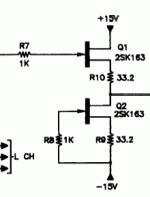
Hafler Series 915 Preamp using JFET buffer (see page 22)
mlloyd1
Hafler Series 915 Preamp using JFET buffer (see page 22)
mlloyd1
Originally posted by BDP
...
I suppose the next step is to put on some connectors and a pot. and have a listen!!
...
BDP
Anyone have any ideas for sockets for the K389? I'd like to build a little test fixture to switch them in and out, in order to find a pair with lowest DC offset. I had thought of individual pin sockets that come in snap off strips, but is there anything else that would be quicker?
Also, John Curl mentions adjusting the lower resistor for minimum offset. By how much typically would I need to adjust from the 10ohm value? Is a pot feasable?
Finally, since I use vishay VTA52 series for the series element in my passive pot setup, I can see that I should use the same for the upper element in the buffer, as it is directly in the signal path. How much of an effect on the sound does the lower resistor have? The vishay's are obviously very expensive.
Thanks,
RonS
One more question, the Hafler schematic that mloyd1 refers to shows a 1k resistor from the gate to the -V supply on the current source, while John Curl and Erno Borbely show the gate connected directly to the -V supply. What effect does the 1k resistor have in the Hafler circuit?
RonS
RonS
The general idea is for both jfets to be configured as similarly as possible to minimize offset and distortion. Look at the gate lead for the signal input jfet...
mlloyd1
mlloyd1
.... What effect does the 1k resistor have in the Hafler circuit?
RonS
Attachments
I think that the extra 1K resistor is a useless oversight. All it adds is extra noise. In some exotic application, or with mosfets, it could be useful, but 1K is still a pretty high value. The 1K resistor adds 4 nV/rt Hz noise to the input of the fet current source. This seems to be a carry-over from transistor circuits, where the significant base current could create an offset, if the two active devices are not equally loaded. With fets, this is not important.
I have been checking the sonic consequences of the usage of the gate stoppers on the JFETs a few times. This might be surprising (was to me at least), but soundwise I found them to be more important on the current source JFETs than on the signal JFETs. Again, might be quite logical if it is considered the fact that in reality we never use zero impedance signal source. So, they almost surely benefit of some bandlimiting. Btw, I never thought (nor I think now) that usage of these two gate stoppers is related.
Pedja
Pedja
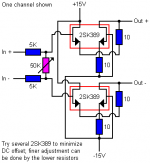
john curl said:My follower suggestion, which runs counter to what I am known for by Erno Borbely, I have found to be almost perfect for most applications. It is simple, direct coupled, low distortion with a relatively high impedance load, quiet, small in surface area, and self limiting, so that it doesn't break easily.
After reading this thread, I'm still not sure what exactly jon curl's circuit suggestion is. Would someone kindly post a schematic?
Like this?
I'm interested in using this as a buffer after a passive balanced volume control. What's the best way to do this? Would I wire each of the four balanced outputs of a balanced stereo volume control to a separate buffer?
Also, I think there was a schematic around diyaudio to only use a stereo attenuator for two balanced channels (resistors in series with inverting and non-inverting, followed by the attenuator in between), but I don't think it had constant input impedance...does anyone remember it?
Attachments
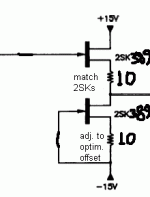
That's the schematic. You don't have to match the fets, because the k389 is a dual fet (2 fets on 1 substrate). You might want to test a few fets though, to find the one with the lowest dc offset.
I'm also planning on using the follower after a volume control, but mine is single ended, with a fixed series resistor and variable shunt pot. Neither the input or output impedance is fixed with this arrangement, one reason to use the follower.
RonS
I'm also planning on using the follower after a volume control, but mine is single ended, with a fixed series resistor and variable shunt pot. Neither the input or output impedance is fixed with this arrangement, one reason to use the follower.
RonS
This is what I was thinking. Is the resistance at input too large for the JFET input capacitance, causing roloff? I was thinking of these values to get a 10K minimum input impedance.
What would be a better way to do it? I plan to use this as a volume control between a DAC and Aleph-X.
Also, how much current should the power supply for this be capable of?
What would be a better way to do it? I plan to use this as a volume control between a DAC and Aleph-X.
Also, how much current should the power supply for this be capable of?
Attachments
Turn the chip upside down Unk
Seems to me that you might might be better off putting the two current sources in one 389 and the two followers in the other one. ( yes I have a couple of reasons)The Idss between the two pairs does not have to be identical. Use the device with the lowest Idss for the current sources and parallel each 10 ohm resistor with another resistor or pot for zero offset. I expect JC to be along in awhile to dope slap me for the suggestion
Seems to me that you might might be better off putting the two current sources in one 389 and the two followers in the other one. ( yes I have a couple of reasons)The Idss between the two pairs does not have to be identical. Use the device with the lowest Idss for the current sources and parallel each 10 ohm resistor with another resistor or pot for zero offset. I expect JC to be along in awhile to dope slap me for the suggestion
- Status
- This old topic is closed. If you want to reopen this topic, contact a moderator using the "Report Post" button.
- Home
- Amplifiers
- Solid State
- Borbely Fet Follower / HarryHaller?