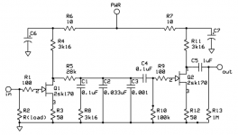
So, I'm building that JFET circuit for a friend of mine, and I ordered out for parts just for fun. I went with the real 2SK170s and as I'm stuffing the board, a little voice tells me to check the pinout of the Toshibas. If I'm reading this mess right, the drain, pin 1, U1, is supposed to tie to R5 and R4, but on my board, if I orient the JFET as it is on the silkscreen, pin 1 will be tied to ground through R3. Looking at several old boards on Images shows the transister reversed, or the right way. I'm confused. Can anyone tell me if this is a known mistake?
Attachments
![IMG_0477[1].jpg](/community/data/attachments/696/696794-5bd29eaffe6f41ed4b99e7005bda263c.jpg)
Here is the correct orientation.
2SK170 pdf, 2SK170 description, 2SK170 datasheets, 2SK170 view ::: ALLDATASHEET :::
2SK170 pdf, 2SK170 description, 2SK170 datasheets, 2SK170 view ::: ALLDATASHEET :::
- Status
- This old topic is closed. If you want to reopen this topic, contact a moderator using the "Report Post" button.