Is it possible to incorporate the sot23 pad layout for an SMD inside or alongside the pad layout of the through hole To92 device?
A GDS (or SDG) To92 pin out is the most common for jFETs. Only the the 2N devices gave the Source as the middle pin.
A sot23 is 1=S, 2=D, 3=G and pin3 is the one on the other side of the package. Surely we just rotate the smd 130degrees to align the pads of both packages.
If this is possible (it does not create any additional PCB area) then we can incorporate both SMD & To92 pads for every transistor location.
Andrew, yes for tH board this should not be a problem.
Yes, this is exactly what I had in mind concerning layout. I like footprints for big 10uF output caps too!
Keeping an eye on this project with interest.
What would be great is a small, low cost board that can be mounted on the back of the pot.

What would be great is a small, low cost board that can be mounted on the back of the pot.
Hi,
a dimensioned Bonsai ready for layouting in either TH or SMD style, with suggestions about devices, power supply range, etc. had been shown in #12, #29 and finally #79.
Unfortunately though, it seems no one really read thoroughly and wasted a thought
And now the Bonsai has become a Borbely, a simple two JFET Buffer 🙄
BTW: with matched JFETs and spending the upper JFETs the same source resistors as the lower JFETs, the output cap could be omitted with alltogether.
You´re really a funny bunch, guys 😀
jauu
Calvin
Guys, I already laid the board out. I will order this week 2 for testing.
I've written up an article as well, but can only publish after I test the board. ( gotta get it 100% right ya know!)
I will post up the layout and schema later tonight.
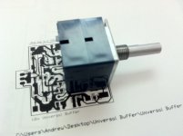
I designed it for an Alps RK27. The board measures 25mm x 48mm and sits on the Alps pot directly.
I've written up an article as well, but can only publish after I test the board. ( gotta get it 100% right ya know!)
I will post up the layout and schema later tonight.
I designed it for an Alps RK27. The board measures 25mm x 48mm and sits on the Alps pot directly.
Hi,
a dimensioned Bonsai ready for layouting in either TH or SMD style, with suggestions about devices, power supply range, etc. had been shown in #12, #29 and finally #79.
Unfortunately though, it seems no one really read thoroughly and wasted a thought
And now the Bonsai has become a Borbely, a simple two JFET Buffer 🙄
BTW: with matched JFETs and spending the upper JFETs the same source resistors as the lower JFETs, the output cap could be omitted with alltogether.
You´re really a funny bunch, guys 😀
jauu
Calvin
Yes you are right Calvin, it is quite possible to get the offset very low. But the FETs need to be well matched - I think dual LSK489 would be good here but they are hard to get and without the cascode, you need low input capacitance. Other option is a trim pot, but I tried to avoid that.
This design does not need matched FETs because the lower FET sets the source current and is sized to fall below the worst case Idss
No originality claimed for the circuit (originally published in 1960s I believe) and indeed Borbely and Pass (B1buffer) are very good designs. Hopefully though, this one is very compact and uses a high quality pot. Sims indicate very low distortion, as reported by NP and EB.
Last edited:
That's a nice pot Ranchu32.
Can you send me the link to the mouser data sheet page? Not promising, but I could do a second layout for that pot.
Can you send me the link to the mouser data sheet page? Not promising, but I could do a second layout for that pot.
No at all, Calvin.Unfortunately though, it seems no one really read thoroughly and wasted a thought
(nanos gigantum humeris insidentes)
Tschüß
I designed it for an Alps RK27. The board measures 25mm x 48mm and sits on the Alps pot directly.
Yeah! 😀
That's a nice pot Ranchu32.
Can you send me the link to the mouser data sheet page? Not promising, but I could do a second layout for that pot.
Here's the link Bonsai: RK09L12D0A1T ALPS | Mouser
But the way you have designed it for the RK27 is even better!
The PCB is designed and the article has been written.
But Inhave not ordered the PCBs yet.
I need to order some for another project shortly, then I will order some boards, build and test.
Note: it's SMD
But Inhave not ordered the PCBs yet.
I need to order some for another project shortly, then I will order some boards, build and test.
Note: it's SMD
Is this (post#100)the final pcb under test?The PCB is designed and the article has been written.
But Inhave not ordered the PCBs yet.
I need to order some for another project shortly, then I will order some boards, build and test.
Note: it's SMD
Thimios.
QUOTE=Bonsai;3963865]...
Note: it's SMD[/QUOTE]


Mmmm, looks like mostly 805, I can handle that. Just no 603! Those ssip me off! 😉


Note: it's SMD[/QUOTE]
Mmmm, looks like mostly 805, I can handle that. Just no 603! Those ssip me off! 😉
Last edited:
I did complete the layout but never built it so was reluctant to publish the board in case there were errors.
I can later today attach the write-up.
I am moving now so digging the layout up will have to wait.
The smallest SMD size was 1206. These are very easy to put down but YOU MUST USE A FINE TIP SOLDERING IRON, 0.8 mm solder and a pair of fine tipped tweezers
I can later today attach the write-up.
I am moving now so digging the layout up will have to wait.
The smallest SMD size was 1206. These are very easy to put down but YOU MUST USE A FINE TIP SOLDERING IRON, 0.8 mm solder and a pair of fine tipped tweezers
- Status
- Not open for further replies.
- Home
- Source & Line
- Analog Line Level
- Bonsai's practical buffer