Just got back from a Hamfest, a guy was selling uA741's, NOS, about 5x the going rate for an NE5534 🙂
Jan
Jan
Kypton V2, way to go OS, you rock!! and I see Terry and others as a loyal followers, maybe I will join the ranks one day.
Just got back from a Hamfest, a guy was selling uA741's, NOS, about 5x the going rate for an NE5534 🙂
Jan
Did you buy some?
Just got back from a Hamfest, a guy was selling uA741's, NOS, about 5x the going rate for an NE5534 🙂
Jan
Are the NOS 741's supposed to sound better than the ones currently available? Ha, ha.
Cheers,
Bob
I here Radio Shack has filed for chapter 11. All I ever saw there was 1970's stock of parts.
I'm not sure all the parts were new though. So UOS. Lots of uA741. I had a guy there try to sell me a 741 for a an open collector voltage comparator. Claimed he was an engineering student, so he should know.
I'm not sure all the parts were new though. So UOS. Lots of uA741. I had a guy there try to sell me a 741 for a an open collector voltage comparator. Claimed he was an engineering student, so he should know.
Are the NOS 741's supposed to sound better than the ones currently available? Ha, ha.
Cheers,
Bob
For best sound you must use the very oldest 14 pin ceramic packaged 741's. Fairchild is best but Motorola is a close second.
Attachments

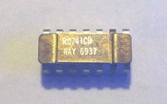
And here another 741 in a 14 pins cerdip: a golden oldie from Raytheon.
Cheers, E.
Now there's the one that actually cost $75.
I bought a couple of them more than 40 years ago, so I can't remember what I've paid for them. Anyhow, in those days it was far less $75.
Cheers, E.
Cheers, E.
I am getting ready to build the power amp and I have to refresh what I put into the pcbs before I dropped everything due to a contracting job. I designed my front end with complementary IPS and push-pull VAS similar to Fig 7.8 in page 137 with added darlington VAS. I was thinking this circuit potentially have large offset drift problem. Particularly it get a lot worst when you have higher value degeneration resistors on the LTP.
I did the simulation to proof my concern. Attached is my LTSpice asc file. You can play with the values. My worst concern is the imbalance between the two current sources at the tails of the two complementary LTPs. You'll find it is hard to match the two current sources unless you are careful in designing it. I tried changing one side from 2mA to 1.5mA, I got over 100mV offset at the output even when I use AC couple on the closed loop feedback. If you use DC closed loop, it will be 100mV times the DC gain which is usually about 20, that will be 2V at the output.
I know the degeneration is important as explained in Fig.3.3 in page 56. The problem is when you have degeneration, you only get rid of the mismatch problem of the LTP itself. The gain of the LTP is so low that any imbalance in the following circuit needs a lot of voltage at the input of the LTP to correct the mismatch. There lies the problem. I don't see a good way to eliminate this short of making sure the current source match and not drift, every the VAS transistors need to be matched as difference in Vbe will cause offset problem. Other than that, the lower the degeneration resistors, the better the offset performance.
If anyone has solution short of lowering the resistor value or painstakingly matching the circuit, I am all ears.
In my asc file, I have two identical circuits except the degeneration resistors. If you change one side to all 0ohm, the offset improves a lot.
Attachments
Last edited:
higher value degeneration reduces the gain and makes the gain less dependent on the differences between the transistors. That to me means degen improves the drift in offset voltage.I am getting ready to build the power amp and I have to refresh what I put into the pcbs before I dropped everything due to a contracting job. I designed my front end with complementary IPS and push-pull VAS similar to Fig 7.8 in page 137 with added darlington VAS. I was thinking this circuit potentially have large offset drift problem. Particularly it get a lot worst when you have higher value degeneration resistors on the LTP.
The output offset is the Difference in Vbe between the two input transistors plus the difference in resistor voltage drops.I did the simulation to proof my concern. Attached is my LTSpice asc file. You can play with the values. My worst concern is the imbalance between the two current sources at the tails of the two complementary LTPs. You'll find it is hard to match the two current sources unless you are careful in designing it. I tried changing one side from 2mA to 1.5mA, I got over 100mV offset at the output even when I use AC couple on the closed loop feedback. If you use DC closed loop, it will be 100mV times the DC gain which is usually about 20, that will be 2V at the output.
I know the degeneration is important as explained in Fig.3.3 in page 56. The problem is when you have degeneration, you only get rid of the mismatch problem of the LTP itself. The gain of the LTP is so low that any imbalance in the following circuit needs a lot of voltage at the input of the LTP to correct the mismatch. There lies the problem. I don't see a good way to eliminate this short of making sure the current source match and not drift, every the VAS transistors need to be matched as difference in Vbe will cause offset problem. Other than that, the lower the degeneration resistors, the better the offset performance.
If anyone has solution short of lowering the resistor value or painstakingly matching the circuit, I am all ears.
In my asc file, I have two identical circuits except the degeneration resistors. If you change one side to all 0ohm, the offset improves a lot.
If the resistors are matched and the resistor currents are matched then the drift in offset at the output CANNOT be dependent on the resistor values.
The drift in output offset is due to the Vbe change as the two devices warm up.
If the two devices operate at the same current Ie and at the same voltage Vce then they dissipate the same power Pq.
Thermally couple the two transistors and the drift in output offset becomes very small.
It is down to ensuring matched resistors, matched currents and matched Vbe/hFE transistors in the input LTP.
Mis match in the second LTP does affect the currents in the input LTP. This does increase output offset, but it is a secondary effect. It's not the second LTP that creates the offset, It's the difference in currents injected into the input LTP that creates the offset.
Good matching of the second stage devices AND much high gain devices will improve this secondary offsetting effect.
No
This has nothing to do with Vbe mismatch of the LTP. Do the simulation. You change the tail current of one of the current source, you create offset. Read my post again.
In fact, the 300ohm degenerate resistor has all but eliminates the Vbe difference of the LPT input transistor. It's the low gain of the stage that require large output offset to balance back the current between the upper and the lower half of the VAS transistors.
Last edited:
I am getting ready to build the power amp and I have to refresh what I put into the pcbs before I dropped everything due to a contracting job. I designed my front end with complementary IPS and push-pull VAS similar to Fig 7.8 in page 137 with added darlington VAS. I was thinking this circuit potentially have large offset drift problem. Particularly it get a lot worst when you have higher value degeneration resistors on the LTP.
I did the simulation to proof my concern. Attached is my LTSpice asc file. You can play with the values. My worst concern is the imbalance between the two current sources at the tails of the two complementary LTPs. You'll find it is hard to match the two current sources unless you are careful in designing it. I tried changing one side from 2mA to 1.5mA, I got over 100mV offset at the output even when I use AC couple on the closed loop feedback. If you use DC closed loop, it will be 100mV times the DC gain which is usually about 20, that will be 2V at the output.
I know the degeneration is important as explained in Fig.3.3 in page 56. The problem is when you have degeneration, you only get rid of the mismatch problem of the LTP itself. The gain of the LTP is so low that any imbalance in the following circuit needs a lot of voltage at the input of the LTP to correct the mismatch. There lies the problem. I don't see a good way to eliminate this short of making sure the current source match and not drift, every the VAS transistors need to be matched as difference in Vbe will cause offset problem. Other than that, the lower the degeneration resistors, the better the offset performance.
If anyone has solution short of lowering the resistor value or painstakingly matching the circuit, I am all ears.
In my asc file, I have two identical circuits except the degeneration resistors. If you change one side to all 0ohm, the offset improves a lot.
Hi Alan,
This is reminiscent of the problem with Randy Slone's circuit, except that he uses current mirror IPS loads instead of resistor IPS loads. Current mirror loads make matters much worse as far as defining VAS idle current.
This is just my first impression, and is not well thought-out.
Cheers,
Bob
"If anyone has solution short of lowering the resistor value or painstakingly matching the circuit, I am all ears."
I don't know of any solution for this kind of circuit (fig. 7.8) I would say forget it and have a look at fig. 7.10. This one should be more stable.
Cheers, E.
I don't know of any solution for this kind of circuit (fig. 7.8) I would say forget it and have a look at fig. 7.10. This one should be more stable.
Cheers, E.
Last edited:
Yes, current mirror loads at the collector of the LTP is much worst as I did the simulation. Offset gets better if the degenerate resistors are reduce because the gain of the LTP increase and does not need a lot of offset voltage from the output to balance the VAS.Hi Alan,
This is reminiscent of the problem with Randy Slone's circuit, except that he uses current mirror IPS loads instead of resistor IPS loads. Current mirror loads make matters much worse as far as defining VAS idle current.
This is just my first impression, and is not well thought-out.
Cheers,
Bob
The question is really what is the optimal value of the degenerating resistors. Lower the value improve offset, but too low value increase distortion. I wonder for 2mA tail current, what is the minimum value I can get away since the dominant source of distortion in a power amp is from the OPS( well unless the IPS is really screwed up!!).
Last edited:
Yes, current mirror loads at the collector of the LTP is much worst as I did the simulation. Offset gets better if the degenerate resistors are reduce because the gain of the LTP increase and does not need a lot of offset voltage from the output to balance the VAS.
The question is really what is the optimal value of the degenerating resistors. Lower the value improve offset, but too low value increase distortion. I wonder for 2mA tail current, what is the minimum value I can get away since the dominant source of distortion in a power amp is from the OPS( well unless the IPS is really screwed up!!).
I think that the problems created by this kind of circuit manifest themselves as both dc offset and VAS standing current (maybe think of it as differential-mode and common-mode problems, respectively). With regard to IPS degeneration, it may be in the damned-if-you-do and damned-if-you-don't category.
Reducing IPS degeneration and increasing IPS gain may reduce DC offset for the reasons you cite, but that approach seems like it may just be covering up the underlying root cause.
It is a little scary because there are many amplifiers out there that use essentially this topology (and with resistor load instead of current mirror load).
Cheers,
Bob
Hi Guys
"Scary" seems like the wrong term - "appropriate" is more accurate, I think.
Comp-diff inputs work best with resistive loading. Open-loop gain can be maximised in other ways and having the diff amp sides balance is also not a huge problem or technical hurdle. Imperious writing such as by Self would make one believe that there is no other way to do things than to cluster the circuit with mirrors and current sources. World-class amplifiers make do without those add-ons.
An easy point to overlook in trying to reduce DC offset is simply to have the base circuit impedances be equal. In the sim, the voltage source at the input often feeds the input base at zero impedance. Even if you leave in a base-stop or LP filter the impedance driving this side of the diff will be much lower than the feedback side and this always results in DC offset. Generally, the base-leak on the input side should equal the series-feedback resistor on the other side, assuming noninverting function. For an inverting amp, one base is grounded and the feedback resistor values should be made as low as possible (should be anyway).
In the sims I've made and physical amplifiers I've built over the years, DC offset has never been an issue. The real amps had no offset that my meter could resolve, so well below 1-2mV. I've never needed a servo, since after all, the whole amp is a servo.
Have fun
Hi Guys
"Scary" seems like the wrong term - "appropriate" is more accurate, I think.
Comp-diff inputs work best with resistive loading. Open-loop gain can be maximised in other ways and having the diff amp sides balance is also not a huge problem or technical hurdle. Imperious writing such as by Self would make one believe that there is no other way to do things than to cluster the circuit with mirrors and current sources. World-class amplifiers make do without those add-ons.
An easy point to overlook in trying to reduce DC offset is simply to have the base circuit impedances be equal. In the sim, the voltage source at the input often feeds the input base at zero impedance. Even if you leave in a base-stop or LP filter the impedance driving this side of the diff will be much lower than the feedback side and this always results in DC offset. Generally, the base-leak on the input side should equal the series-feedback resistor on the other side, assuming noninverting function. For an inverting amp, one base is grounded and the feedback resistor values should be made as low as possible (should be anyway).
In the sims I've made and physical amplifiers I've built over the years, DC offset has never been an issue. The real amps had no offset that my meter could resolve, so well below 1-2mV. I've never needed a servo, since after all, the whole amp is a servo.
Have fun
The thing here is that the schematic that was shown above was one with resistive loading of the IPS.
You are largely correct about the relationship of the input return and feedback resistances in minimizing offset. However, your suggestion that the input side return resistance is usually very low is only true for DC coupled amplifiers. For most amplifiers, which are ac coupled at the input, the base return resistor is normally a fairly high-value resistor (10k - 50k) and should indeed be ideally the same value as the feedback resistor.
Indeed, this creates a bit of a conflict or trade-off in many conventional designs, since keeping the impedance of the feedback network small (for noise and other reasons) tends to force the input return resistor small, creating a heavier load on the source preamp and requiring a larger coupling capacitor.
There are some ways around this, including the use of a dc servo and other approaches, such as padding the feedback-side dc resistance with a bypassed resistor in series with the base.
Cheers,
Bob
- Home
- Amplifiers
- Solid State
- Bob Cordell's Power amplifier book