Greetings everyone!
I am in the process of doing a senior project and mine just so happens to include a few audio amplification portions. I've been gradually generating the blue prints for it until I found myself coming to a grinding halt when I came to the analysis portion of a Class AB amplifier. The reason I came to a grinding halt is because the analysis methods I have for BJTs appear to be inappropriate for AB amplifiers. To gain an idea of where I am coming from, allow me to walk you through a simple analysis of a Class A amplifier. This will demonstrate the techniques and methods I am used to using.
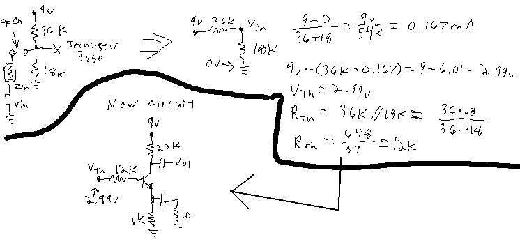
Now first, I would do the DC analysis of the transistor. This means to first remodel the circuit where the following rules apply;
* Capacitors are opened - assume there is no connection across them
* Inductors are shorted - assume the inductor is short circuit
* AC voltage sources are shorts to ground
* AC current sources are opened in the same way capacitors are.
Now the first thing we would need to do is find the voltage going into the base. So, I will create a thevinin equivalent of the base circuit.
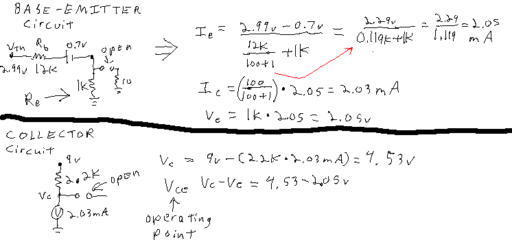
Now that I have a simple equivalent circuit I can figure out the DC collector current which I need for AC analysis. I know that the Base-Emitter current determines the collector current so I'll first analyze the Base Emitter then I'll analyze the collector. We'll assume Beta (or hfe if you please) is 100...
So now that we know the DC portion is sound and we also have the collector current we can figure out the AC portion. The AC modeling is 'hacky' at best so I'll just show each section separately. First and for-most we need Rint and hie. Before I forget, here are the AC rules I know of;
* Inductors are opened - assume there is no connection across them
* Capacitors are shorted - assume the inductor is short circuit
* DC voltage sources are shorts to ground
* DC current sources are opened in the same way capacitors are.
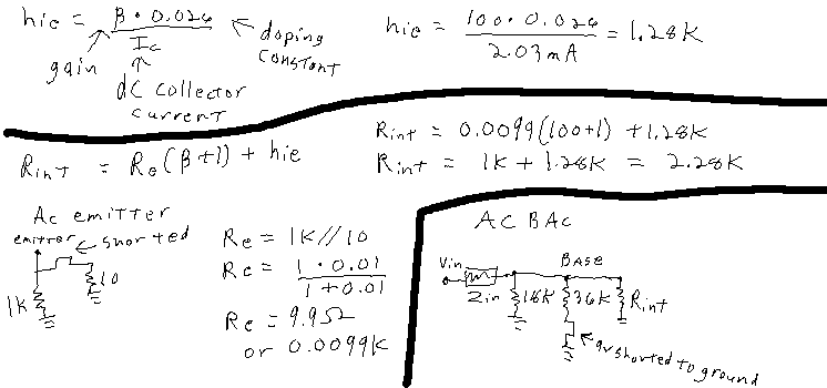
Now that we have Rint and hie, we can find the input losses, the collector output(V1) and the emitter output(V2). Lets first clean up the base. It's circuit is a mess. Let's also assume at this point that our input is 50mV peak-to-peak and our input impedance is 10K.
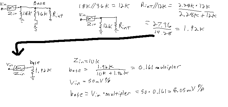
Now that I have the actual input voltage and Rint I can find the collector output voltage gain and the emitter output voltage gain.
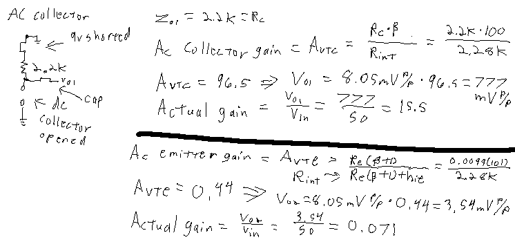
So as we can see, the collector gain is 15.5 and the emitter gain is 0.071. This would be a viable Common-Emitter amp for voltage gain but a very poor choice for an Emitter-Follower for current gain with selected Input. As you may have noticed; the Avte equation can never exceed 1 unless you intentionally mess it up.
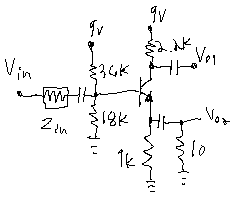
Now that I've demonstrated how I approach transistor analysis, I bring to you a standard AB amplifier I see frequently;
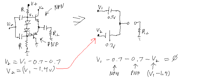
As you can see, the voltage difference from the base of the NPN to the PNP becomes 0v. Without a voltage difference between two points, no current flows. With no current flow from Base to Emitter, the Collector current becomes 0 Amps. When the collector current is 0 Amps, hie becomes infinity as does Rint. This messes up all calculations I know.
How the hell does this thing work? What sort of analysis do you need to figure out what the current flow is? If anyone could explain how you would approach this and what formulas you'd use, that'd be great! My feelings about AB amplifiers at the moment are:
 Any help would be greatly appreciated! Thanks!
note; I apologize in advance if the forums auto parses this post and removes line breaks. Sometimes forums do that randomly. This one does it in the preview so I can't tell if it will show up poorly or not.
edit: Okay I fixed the line break problem...
I am in the process of doing a senior project and mine just so happens to include a few audio amplification portions. I've been gradually generating the blue prints for it until I found myself coming to a grinding halt when I came to the analysis portion of a Class AB amplifier. The reason I came to a grinding halt is because the analysis methods I have for BJTs appear to be inappropriate for AB amplifiers. To gain an idea of where I am coming from, allow me to walk you through a simple analysis of a Class A amplifier. This will demonstrate the techniques and methods I am used to using.
Now first, I would do the DC analysis of the transistor. This means to first remodel the circuit where the following rules apply;
* Capacitors are opened - assume there is no connection across them
* Inductors are shorted - assume the inductor is short circuit
* AC voltage sources are shorts to ground
* AC current sources are opened in the same way capacitors are.
Now the first thing we would need to do is find the voltage going into the base. So, I will create a thevinin equivalent of the base circuit.
Now that I have a simple equivalent circuit I can figure out the DC collector current which I need for AC analysis. I know that the Base-Emitter current determines the collector current so I'll first analyze the Base Emitter then I'll analyze the collector. We'll assume Beta (or hfe if you please) is 100...
So now that we know the DC portion is sound and we also have the collector current we can figure out the AC portion. The AC modeling is 'hacky' at best so I'll just show each section separately. First and for-most we need Rint and hie. Before I forget, here are the AC rules I know of;
* Inductors are opened - assume there is no connection across them
* Capacitors are shorted - assume the inductor is short circuit
* DC voltage sources are shorts to ground
* DC current sources are opened in the same way capacitors are.
Now that we have Rint and hie, we can find the input losses, the collector output(V1) and the emitter output(V2). Lets first clean up the base. It's circuit is a mess. Let's also assume at this point that our input is 50mV peak-to-peak and our input impedance is 10K.
Now that I have the actual input voltage and Rint I can find the collector output voltage gain and the emitter output voltage gain.
So as we can see, the collector gain is 15.5 and the emitter gain is 0.071. This would be a viable Common-Emitter amp for voltage gain but a very poor choice for an Emitter-Follower for current gain with selected Input. As you may have noticed; the Avte equation can never exceed 1 unless you intentionally mess it up.
Now that I've demonstrated how I approach transistor analysis, I bring to you a standard AB amplifier I see frequently;
As you can see, the voltage difference from the base of the NPN to the PNP becomes 0v. Without a voltage difference between two points, no current flows. With no current flow from Base to Emitter, the Collector current becomes 0 Amps. When the collector current is 0 Amps, hie becomes infinity as does Rint. This messes up all calculations I know.
How the hell does this thing work? What sort of analysis do you need to figure out what the current flow is? If anyone could explain how you would approach this and what formulas you'd use, that'd be great! My feelings about AB amplifiers at the moment are:
note; I apologize in advance if the forums auto parses this post and removes line breaks. Sometimes forums do that randomly. This one does it in the preview so I can't tell if it will show up poorly or not.
edit: Okay I fixed the line break problem...
Last edited:
First of all, how did you conclude that the voltage between the two bases is zero? There are two happily conducting forward-biased diodes in between (DC wise of course). So the base-emitter junctions should also be forward-biased, don't you think?
Even if it were, however, the stage would still (sort of) work. One of the transistors would start conducting once input voltage had gotten far away from midpoint for them to conduct. This is commonly called class-B operation (though some like Douglas Self have argued that the "dead zone" rather implies class-C).
For the sake of simplicity, connect your input in between the two diodes, assuming current through them always being a good bit larger than signal current.
Further consider the output coupling capacitor a DC level shifter, i.e. a fairly ideal voltage source.
If it makes things easier for you, you can also consider an all DC-coupled version with split positive and negative supplies and both input and load being directly ground-referenced - as is usually the case in practical power amplifiers anyway. Then sweep input voltage from negative to positive rail.
Have you looked at push-pull amplifiers in textbooks (Horowitz/Hill comes to mind) or on the web?
BTW, it's not that easy to make an inductor that isn't a fairly decent low-value resistor at audio frequencies.
I suggest you grab a circuit simulator like LTspice (bog standard small-signal transistors like BC547/557 should do). That has the distinct advantage of not having to work with crude approximations and usually gives you a much better feel of what's going on. Calculations are still useful, of course, like for eyeballing operating points when looking at a schematic.
Last edited:
Nutshell....
Theory says that a SI PN junction forward breakdown is 0.7V but in reality it is more like 0.6V, and it is dependent upon temperature. If you plot the Ic vs Vce curves for each device you can see the AC load line traverses both devices. Each device only conducts 180 degrees of signal so this means that there is a point at where one device turns off and the other turns on. With no bias this would be class B operation, and there would be a large disruption in the output impedance curve around the zero current switching point, IOW lots of crossover distortion. The goal is to have a constant output impedance in order to improve the linearity. This means you need bias. However, too much bias also creates a disruption in the output Z consistency, called Gm doubling, when both devices are on and contribute to the output Z. This is why we compromise and use emitter resistors. The value for the emitter resistor should be about the same as the output transistor's re, or intrinsic resistance at idle current. For most of the AC load line, the output Z will be one emitter resistor. As re from the transistor increases as the Q point approaches the zero current crossover and the other transistor begins to conduct, the two emitter resistors appear parallel and this helps to straighten the output Z function and make it less dependent on the variable goss of the transistors. Also the emitter resistors provide some degeneration feedback allowing for bias stability.
Theory says that a SI PN junction forward breakdown is 0.7V but in reality it is more like 0.6V, and it is dependent upon temperature. If you plot the Ic vs Vce curves for each device you can see the AC load line traverses both devices. Each device only conducts 180 degrees of signal so this means that there is a point at where one device turns off and the other turns on. With no bias this would be class B operation, and there would be a large disruption in the output impedance curve around the zero current switching point, IOW lots of crossover distortion. The goal is to have a constant output impedance in order to improve the linearity. This means you need bias. However, too much bias also creates a disruption in the output Z consistency, called Gm doubling, when both devices are on and contribute to the output Z. This is why we compromise and use emitter resistors. The value for the emitter resistor should be about the same as the output transistor's re, or intrinsic resistance at idle current. For most of the AC load line, the output Z will be one emitter resistor. As re from the transistor increases as the Q point approaches the zero current crossover and the other transistor begins to conduct, the two emitter resistors appear parallel and this helps to straighten the output Z function and make it less dependent on the variable goss of the transistors. Also the emitter resistors provide some degeneration feedback allowing for bias stability.
Have you looked at push-pull amplifiers in textbooks (Horowitz/Hill comes to mind) or on the web?
I suggest you grab a circuit simulator like LTspice (bog standard small-signal transistors like BC547/557 should do). That has the distinct advantage of not having to work with crude approximations and usually gives you a much better feel of what's going on. Calculations are still useful, of course, like for eyeballing operating points when looking at a schematic.
Yea, I looked around on the web and checked every circuits book I could get my hands on but usually I see two problems;
1) Almost no source has actual formulas I can use for modeling or analysis
2) The ones that do have analysis formulas only have approximate gains for the entire circuit they present which usually includes 3 to 5 stages. No book or website that I can find show analysis of JUST the AB portion.
What is a circuit simulator?
Nutshell....
Theory says that a SI PN junction forward breakdown is 0.7V but in reality it is more like 0.6V, and it is dependent upon temperature. If you plot the Ic vs Vce curves for each device you can see the AC load line traverses both devices. Each device only conducts 180 degrees of signal so this means that there is a point at where one device turns off and the other turns on. With no bias this would be class B operation, and there would be a large disruption in the output impedance curve around the zero current switching point, IOW lots of crossover distortion. The goal is to have a constant output impedance in order to improve the linearity. This means you need bias... *very useful information*
That's explains why my modeling doesn't work... I imagine I'd need like the datasheet of the transistors I am using before I can modeling them in this situation?
Oh and for future reference, how good are 2N3904 and 2N3906 for audio amplifiers? They are pretty much the only BJT transistors I have worked with throughout my EE classes.
> What is a circuit simulator?
You don't need it. It is a computer program, it tells you numbers, mostly wrong. It does NOT help you understand.
Stick with cocktail napkins. It's how all good electronics is done.
> I imagine I'd need like the datasheet of the transistors I am using before I can modeling them in this situation?
Well, darn. You are already corrupted. Good-on-you for doing it in pencil anyway.
You don't need the datasheet. All transistors are the same, except the stuff that's different. Imagine an infinite transistor, and they cut-off as much as you pay for. A little '3904? A big '3055? Actually there's some tradeoffs. High voltage tends to low Beta. It may be easier to get lower leakage and better Beta in small devices.
> voltage difference from the base of the NPN to the PNP becomes 0v. Without a voltage difference between two points, no current flows. With no current flow from Base to Emitter, the Collector current becomes 0 Amps. When the collector current is 0 Amps, hie becomes infinity as does Rint.
OK so far. In fact you found a "flaw" in AB, but we'll skip it for now.
Put a signal in. Say 10V. Say load is 10 ohms. One transistor is off, the other one is conducting 1 Amp. The hIE is like 0.03 ohms. That's also the output impedance. The voltage gain is roughly 10/10.03 or 0.997.
So an AB stage WILL smack a speaker pretty good.
> When the collector current is 0 Amps
Yeah, that's a problem.
But does a transistor's current ever reach dead-zero? Say 0.6V gives 1mA. Then 0.64V is 0.1mA, 0.48V gives 0.01mA, 0.42V gives 0.001mA, and 0.3V gives 0.000,01mA. NOT "zero".
But of course if load is 10 ohms and idle current is say 1mA, the gain for incredibly small signals is 0.25, but 0.99 for large signals. "Crossover Distortion".
If you dig into practical AB amps, they always (usually) twiddle those diodes so the idle voltage is high enough to get the output devices well above "zero current", above "too-small current". This is fussy, so there's ~~1-ohm emitter resistors. If output devices try to carry large idle current, resistor drop fights it.
You have good chops for "linear" design, where device current is always "medium". In this zone, many simplifications and approximations are valid-enough. You can even carry these to very-large swings, class-A Power amplifiers. If you idle at 30mA, and swing 3mA to 57mA, you can compute hIE swinging 10 ohms to 0.5 ohms, and sketch the bent waveform. But when the signal swing is 100 times the idle, you need to think different.
So... What I gather so far is that transistors don't have a sharp on/off switch at exactly 0.7v. Instead they can begin to switch on at significantly lower voltages. This changes the playing field so to speak.
This also makes me think; Wait, so if the NP junction drop in a transistor isn't locked at 0.7v, what about diodes? Do they start conducting before you reach 0.7(or before 0.2v if you use schottky diodes)?
It appears these discrete devices are more analog than I expected.
This also makes me think; Wait, so if the NP junction drop in a transistor isn't locked at 0.7v, what about diodes? Do they start conducting before you reach 0.7(or before 0.2v if you use schottky diodes)?
It appears these discrete devices are more analog than I expected.
So... What I gather so far is that transistors don't have a sharp on/off switch at exactly 0.7v. Instead they can begin to switch on at significantly lower voltages. This changes the playing field so to speak.
This also makes me think; Wait, so if the NP junction drop in a transistor isn't locked at 0.7v, what about diodes? Do they start conducting before you reach 0.7(or before 0.2v if you use schottky diodes)?
It appears these discrete devices are more analog than I expected.
Absolutely. This is solid state amplification. Transistors are very convenient amplifiers but in fact they are not very good at it. They are much more happy being switches, on or off. It’s not hollow state.😛 When you start to operate within the ‘linear’ region the basics of BJT operation is only the surface. BJT’s in particular have peculiar distortions such as the Early effect. This represents a change in the curves of Ic vs. Vce. Since the current gain is somewhat dependent on Vce and Vce modulates with the signal, this small change in output Z creates a distortion. You have to look at the curves for a transistor to determine the Early Voltage. Simply plot the lines of the Ic vs Vce graph to the common point on the x axis(in quadrant 2) and that is the Early voltage. Don’t be fooled, those datasheets really are useful. Because transistors are really ‘limited’ linear amplifiers and they are cheap it allows you to use cascode circuits and other ways to make the variables that are just part of a transistor’s function more constant.
It sounds like you are a student fishing for fundamentals. Have you taken physics and chemistry in order to understand how and why a PN junction exists and what a depletion region is and how it‘s created? I mean, for example Electronics 101 Lab assignments should show you roughly 0.6Vbe at turn on.
BTW diode Vf is dependent on the current. Some large power diodes my have over 1V foward voltage drop at high currents.
The two Chemistry classes I've taken just explained how chemical reactions take place, how to determine the result of a reaction, the ammount of material which reacts, and other basic chemistry principles. Nothing about silicon or electronics was even mentioned.
The two physics classes I took were strictly newtonian physics, so nothing about electricity was even mentioned.
I've taken Three electronics classes which were labeled as senior level. The topics covered were: Diodes(regular, schottky, and zenor), BJT Class A amps, BJT Diff Amps, JFET/MOSTFET switching properties, Op-Amps, buttersworth/bessels/chevychev filters, TTL/CMOS digital logic chips, Voltage Comparators, Voltage Regulators, Crowbar regulating, 555 Timers, Instrument Amps with Op-Amps, Summing Amps with Op-Amps, AC to DC rectifiers, Powerfactor Correction, Boost/Buck/SEPIC/Cuk/Flyback switching power supplies, Feedback controllers, Steinmetz transformer modeling, and Three phase circuits/transformers.
Since they cover A LOT of material they simply show us the basics of each topic, test us, and move on. They don't have time to spend that long on any topic so consequently I don't know a lot of the nitty gritty details. Like with BJTs, other than what I showed you guys all they mentioned is that in saturation mode the collector is no longer modeled as a current source, but a 0.2v battery.
I guess you could say I am fishing for the details left out. I can't reference a book since the same professor taught all 3 classes and didn't use a book, but just his own notes. The BJT transistor lab was building a Common Emitter and Emitter follower, noting the gains, changing the input for another data set.
Edit; By the way, when I used 0.6v for analysis/modeling and actually threw the circuit together on a bread board for testing it worked and produced results fairly close to what I calculated. I just used arbitrarily selected parts. AB amps are pretty interesting in that they don't constantly draw crap tons of power like Class A Amps. I noticed that the current drawn by the AB amp varied far more than with the Emitter Follower A Amp.
Last edited:
You need to understand that the current through a BJT varies as the exponential of Vbe, with a scaling factor of around 40mV (see Ebers-Moll model). This means that much more than 0.6V will cook the transistor through overcurrent, and much less than 0.6V will make it look 'off'. Similar for a diode.
The book you need is by Horowitz and Hill: "The Art of Electronics". You can't be a serious electronics student without reading it.
The book you need is by Horowitz and Hill: "The Art of Electronics". You can't be a serious electronics student without reading it.
Your mostly right, but you need to use the Ebers-Mole transistor model for ac analysis. You first example incorectly includes the effect of the emiter resistor (10 ohm) on the transistor input impedance. ( it increase the input Z by Hfe*RE or about 1k). And as already stated, an AB amp needs to be analysed a half cycle at a time. Most AB amps have emitter follower outputs, which have a V gain very close to 1. (but large current gains).
I totally disagree. The numbers are mostly right ( if you know what your doing) and seeing a circuit operate (even virtually) can help you gain understanding. Sure its better to build a circuit, but most cant afford to set up all the equipment. LTSpice is free and it works. Im not saying it replaces learning the theory with a pencil, Im saying it replaces the lab part of studying electronics ( wich I believe is just as important)
And a lot of great electronics start out in a simulator.
> What is a circuit simulator?
You don't need it. It is a computer program, it tells you numbers, mostly wrong. It does NOT help you understand.
Stick with cocktail napkins. It's how all good electronics is done.
I totally disagree. The numbers are mostly right ( if you know what your doing) and seeing a circuit operate (even virtually) can help you gain understanding. Sure its better to build a circuit, but most cant afford to set up all the equipment. LTSpice is free and it works. Im not saying it replaces learning the theory with a pencil, Im saying it replaces the lab part of studying electronics ( wich I believe is just as important)
And a lot of great electronics start out in a simulator.
So basically you've been taught BJTs in very simplified models (which may very well be OK in practice but does not lend itself to deeper understanding).
Here's another model that tends to be reasonably useful for DC / low frequencies in practice:
A forward-biased transistor's base-emitter junction is a p-n junction much like you find in a silicon diode, which means an exponential relation between B-E voltage and base current. (It "takes off" at around 0.6 V.)
The base current in turn controls collector current by means of current amplification B / h_FE or its well-known small-signal cousin beta. Note that beta is often assumed to be constant. It can be reasonably constant over a certain range, but a transistor datasheet will reveal that it is anything but set in stone. There also is a certain variation of collector current with collector-emitter voltage, the aforementioned Early effect.
If collector-emitter voltage becomes very low, the transistor is saturated and no longer able to source/sink as much current as you'd like. This puts a limit to how close you can get to the supply rails, typically the aforementioned 0.2 V, though the exact value depends on collector current levels.
The Wikipedia article on transistors isn't what I'd call ideally structured, but it does mention the Ebers-Moll model.
Horowitz/Hill seems like a good idea indeed. Here in .de the standard transistor book would be the equally voluminous Tietze/Schenk, which also exists in an English translation though I'm not sure how widespread that would be.
Last edited:
> these discrete devices are more analog than I expected
?? Not discrete versus analog. You could say discrete versus integrated. You could say analog versus digital. However all "digital" devices are analog; we only pretend they work 1/0 because we slam them through the linear zone "very fast".
> transistors don't have a sharp on/off switch at exactly 0.7v
Current doubles for every 20mV.
This is the same as your chemistry where many reactions double in speed every 10 degrees C. It is probably the same at the atomic level but with charge-on-electron as a factor.
Ebers-Moll is good to skim, but really not needed for audio design. You do need to get outside small-signal class A. What happens when voltage or current "hits zero"? It's never really zero, just very-small. Correct interpolation of "Class A" getting smaller and smaller will lead you to a workable result.
> in saturation mode the collector is no longer modeled as a current source, but a 0.2v battery.
There's qualifications on that "0.2V". It is really the difference of the BE and CB diodes. For small currents it may be more like 0.05V. But for "Power" amplifiers we are always caught between big outputs and limited money. In "saturation" there is an Ohmic component and in audio power amplifiers this is usually non-negligible. And in audio we normally do not saturate (OK, we do in our dens, but in testing we try to stay just short of saturation). You can see on the 2N3055 data that there's several Volts C-E at near-saturation.
> I totally disagree. ...seeing a circuit operate (even virtually) can help you
I also advocate slide-rules. A lot of electronics is ratios, and ratios pop-out on the slipstick much better than on a key-calculator. I also say that $1 and $5 screw-ups on breadboard are very effective lessons.
Welp! I just wanna pitch in and add that you've all provided me with with some very useful information. I've made alot of progress in my amp design so far. I learned a hand full of nifty tricks thanks to everyone's input. I feel that my design still needs refinement, but it's come a LONG way since since I first posted this thread.
CBS240, cbdb, PRR, and sgrossklass - you guys in particular provided some great insight.
Personally I believe there is a time and place for most methods and tools. I prefer to do what I can by hand whenever possible. I try not to reach for tools like calculators, (and soon to be simulation software) until I need to. Scratching down designs and calculations on graph paper and then building them up on bread/proto boards is just how I was brought up throughout my career as an EE student. I've only recently been acquainted with maple and matlab and I have mixed feelings about them. Microcap on the other hand seems like it may be a practical tool.
- Status
- Not open for further replies.
- Home
- Amplifiers
- Solid State
- BJT Analysis and Formulas for AB Amplifiers