Yes, the current in the 0.33 ohm equals the current flowing through the output devices. The 'devices' are the four output transistors in question.
When the amp runs with no bias, the current drawn overall is small and so the power supply delivers its maximum voltage. Think of a new battery. It might read 1.65 volts under very light load. Draw a little current and it falls quickly to perhaps 1.55 volts. Draw more and it falls a bit further but then continues to supply the current asked of it. Its a bit like that with power supply.
I wouldn't try and start over running things, fan or no fan because that's asking for trouble imo. You can't make it something it was never intended to be, all you can do is optimise and get it as best as you can within the original design constraints.
Just my opinion, but that's what I would do 🙂
Take the voltage.. Earlier you said 29mV
Divide that by the resistance.. .33ohms
so.. .029V divided by .33ohms = .0878 which is 88mA
I think I'm correct. Thats my formula.
Although I dont see 29mV being a problem. It was recommended earlier to drop it to 25mV. But I think your bias is close enough if your getting 29-30mV from emitter resistor.
It was set to 23.6mv so that'd be 0.0715 or 71.5mA? It's dropped to as low as 20-21mv in use with low mild volume.
Yes, the current in the 0.33 ohm equals the current flowing through the output devices. The 'devices' are the four output transistors in question.
When the amp runs with no bias, the current drawn overall is small and so the power supply delivers its maximum voltage. Think of a new battery. It might read 1.65 volts under very light load. Draw a little current and it falls quickly to perhaps 1.55 volts. Draw more and it falls a bit further but then continues to supply the current asked of it. Its a bit like that with power supply.
I wouldn't try and start over running things, fan or no fan because that's asking for trouble imo. You can't make it something it was never intended to be, all you can do is optimise and get it as best as you can within the original design constraints.
Just my opinion, but that's what I would do 🙂
Thanks for the clarification. I might still tack on some heat sink sections later to help dissipate heat a little better as these can get hot running higher volumes, and a fan wouldn't hurt anyways, to help with longevity, but I'll leave settings alone.
Out of curiosity, I've seen ON SEMI has more modern counterparts to these older style transistors others have mentioned in different threads. Any idea if they'd be an improvement with THD, response, etc?
Older designs often take into account (lets rephrase that), older designs rely on the devices characteristics as part of the whole design. That means that you can't always swap in more modern parts without a bit of a redesign. Typical problems would be an inability to bias the amp correctly because the Vbe (transistor base/emitter turn on voltage) is slightly different due to different manufacturing processes of early devices. There can also be stability issues (oscillation).
Are modern counterparts (not upgrades, just what's offered as either direct replacement or what's traditionally been the next closest alternative) any better than older? Or are they essentially identical? Like my AB gear, one uses Toshiba and other used Motorola. Both have ON SEMI alternatives.
Just wondering if they improved any of the design in the last 40 years through better manufacturing processes? Like 40 years ago, I think 10-20% was common for resistors. Now 1% tolerance are easy to find. Have transistor replacements fared as well? Or are they basically identical?
Just wondering if they improved any of the design in the last 40 years through better manufacturing processes? Like 40 years ago, I think 10-20% was common for resistors. Now 1% tolerance are easy to find. Have transistor replacements fared as well? Or are they basically identical?
Modern transistors use slightly different processes and doping techniques compared to early examples. So a modern On Semi part and modern Motorola will be similar in the production methods used to make them but both very different from early devices from these manufacturers 9well On Semi weren't around but you know what I mean).
A modern power device will be more rugged and have a wider SOAR (safe operating area) than early devices.
LED's are another good example. Modern ones far outshine early ones due to improvements in doping, materials and manufacture and yet they are still from the same family of devices.
Stick to what was originally fitted... if you start changing things without the knowledge of what to look for and what to change to make the new parts work correctly then its asking for trouble.
I was thinking ahead in case one of these (38 year old) transistors eventually fail, along with any possibility of improving THD or added noise being a benefit. As it stands, at least have parts unit with correct pieces.
ON SEMI was branched off of Motorola, so technically they are the same company. When I redo my 600LX (still no comments in live band 🙁 ) I'll go with all ON SEMI so everything matches.
Was just wondering if anyone has done a back to back with the early stuff vs. it's modern replacement, if any improvement in sound was audible or changes occurred.
Actually, I should just email them and see what they say.
Looked a little closer at at layout, and from what I can tell, the lower right corner leg on left channel pot, and lower left leg of right channel pot (didn't realize at first that actually mirror each other until setting bias, so opposite corners) hit a resistor, which then goes straight to the center pin (base) of a MN2 6554 (think it's actually a 2N6554 that looks like this: http://alltransistors.com/pdfview.p...2n6553_2n6554_2n6555_2n6556.pdf&dire=_central) and also has a 68nF (might be pF) ceramic that jumps to something else and a tiny NPN left leg (might be emitter lead??) lead?. All .33 emitter resistors output to the left center pins of their respective 3055/2955's if looking at the round disc back side with legs pointing away while staring at the printed label. So from that point of view, it has center left, center right leads, then the outer casing all have a wire connected. All outer casings on all 4 are same orange color wire.
From that info, and pics provided, does this sound like a CFP still?
From that info, and pics provided, does this sound like a CFP still?
Last edited:
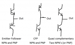
Three common output stages. Forget where the 0.33 ohms are. Look how the collectors are wired and look at the device types. You have an NPN/PNP so that noarrows it down to EF or CFP. If the speaker output is from the collectors (middle leg of the 3055/2955) then its CFP. If its from the emitters its EF.
Attachments
Sorry, that illustration doesn't help as I don't what's what there.
Looking at the parts amp board, and this .pdf link from ON SEMI http://www.onsemi.com/pub_link/Collateral/2N3055-D.PDF (scroll at very bottom for image that can be increased in size)
that shows the 3055's outputs, if I follow no.2 (emitter) which is the yellow wire on the pics I posted further back, it only feeds through one .33 emitter resistor, which is linked directly to the traces that feed the "out" on each channel along with connecting to a lead on a bias pot.
This sound like an EF setup then? If so, are the values I biased at still acceptable?
It looks like EF looking at the picture, lol, but looking at pictures is not really 'engineer speak' though.
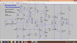
The bias values I mentioned should be fine and I wouldn't go any higher given the size of the heatsink. This shows an EF output stage with 0.22 ohm resistors. Yours should be similar in basic topology. The output transistors are the right hand pair. Your 3055 would be the top and the 2955 the bottom.
The bias values I mentioned should be fine and I wouldn't go any higher given the size of the heatsink. This shows an EF output stage with 0.22 ohm resistors. Yours should be similar in basic topology. The output transistors are the right hand pair. Your 3055 would be the top and the 2955 the bottom.
Attachments

I was following the traces on the board bottom. the no.2 pin off the 3055 is emitter, and after it flows through the .33 emitter resistor, junctions to a large trace section that connects to 1 of 2 of the board "out" posts (one "out" per channel), while also being connected to a leg of the bias pot. The board has audio "in" posts that feed directly from tone board, and these "outs" I think go the speaker channel fuse, which I believe comes back to the front for the speaker A/B/Matrix selector button and a set of cement resistors, before going back to the rear speaker terminals. Matrix ground uses a 3rd cement resistor on the actual power supply board, separate from the 2 independent cement resistors attached to speaker switch board.
BTW, when looking at circuit boards with labeled markings, what does "Q" and also "V" actually stand for?
"VR" represents "variable resistor", right?
Looking at transistor (Q14) in your pic, that's basically the same as the 3055, right? The line with triangle pointing away and feeding the (R20) emitter resistor, that's like my 3055 emitter lead feeding my .33 resistor?
Do you have a non-cropped version of that thumbnail? It only shows right-hand side.
Thanks.
Last edited:
I have designed my own 2n3055/mj2955 amplifiers.
I set the dc offset to as close to zero as possible.
Connect a speaker.
Then I apply a small sine wave to the input while monitoring output with a scope.
I turn the bias up slowly until cross over distortion goes.
I set the dc offset to as close to zero as possible.
Connect a speaker.
Then I apply a small sine wave to the input while monitoring output with a scope.
I turn the bias up slowly until cross over distortion goes.
BTW, when looking at circuit boards with labeled markings, what does "Q" and also "V" actually stand for?
"VR" represents "variable resistor", right?
Looking at transistor (Q14) in your pic, that's basically the same as the 3055, right? The line with triangle pointing away and feeding the (R20) emitter resistor, that's like my 3055 emitter lead feeding my .33 resistor?
Do you have a non-cropped version of that thumbnail? It only shows right-hand side.
Thanks.
Q is often used to denote transistors (also TR is often used). V is usually denoting voltage. Manufacturers often have there own labelling schemes.
The output stage I posted is just a classic Class AB amp. Yours will have similarities although obviously differ in detail.
Attachments
Q is often used to denote transistors (also TR is often used). V is usually denoting voltage. Manufacturers often have there own labelling schemes.
The output stage I posted is just a classic Class AB amp. Yours will have similarities although obviously differ in detail.
Thanks for the clarification.
The image you linked states "Class B"?
Does the line with a triangle on an output transistor denote an emitter lead? Also, does it represent a direction the current is going?
I have designed my own 2n3055/mj2955 amplifiers.
I set the dc offset to as close to zero as possible.
Connect a speaker.
Then I apply a small sine wave to the input while monitoring output with a scope.
I turn the bias up slowly until cross over distortion goes.
What do you mean "until crossover distortion goes"? Is that "goes away"? Or until it appears? Also, with your amps, what's an average norm bias you end up with? And does this crossover distortion occur early or later? Is it actually audible? If so, what does it sound like or rather what effect on sound is noticeable?
Does the line with a triangle on an output transistor denote an emitter lead? Also, does it represent a direction the current is going?
The arrow (which is always the emitter) either points outward for NPN devices or inwards for PNP.
The collector is always the most positive terminal for an NPN and for a PNP its the most negative. You can see how that works just by looking at the diagram. You could say the collector 'collects' current from the supply and the output is 'emitted' by the emitter. Its not quite that simple but you get the idea.
If you are interested in how all this works then click my signature line and have a go at installing LTSpice which is a simulation program. That Class B amp diagram is a simulation which I can post if you want it.
The crossover distortion will probably "go away", as in, not be immediately objectionable when you get around 0.5-1 millvolt acrosss the emitter resistors. It will probably take 30mV or so to get to minimum distortion, but that will probably run too hot. The right answer is somewhere in between.
If I understand this thing correctly, it's an EF. If the green wire coming out of the center goes to the negative rail, that's what it is.
Collector and emitter are carryovers from the tube days. "Emitter" used to be a heated cathode, which actually "emitted" electrons. They "collected" on the plate. Fo a PNP transistor, the charge carriers are "holes", which is a space that an electron can occupy in the crystal lattice. They "travel" the opposite way. The "emitter" emits holes. The arrows point in the direction of conventional current. The whole thing about "conventional current" being backwards is just messed up. I guess nobody wanted to go back and change the sign on all the math they worked out.
Get too many nerds together in a room and they come up with some effed up stuff. And make very bad jokes.
What do you mean "until crossover distortion goes"? Is that "goes away"? Or until it appears? Also, with your amps, what's an average norm bias you end up with? And does this crossover distortion occur early or later? Is it actually audible? If so, what does it sound like or rather what effect on sound is noticeable?
You will see glitches on the sine wave output if crossover distortion is there.
Turn up bias until glitches have gone.
Crossover distortion is audible at low listening levels.
The arrow (which is always the emitter) either points outward for NPN devices or inwards for PNP.
The collector is always the most positive terminal for an NPN and for a PNP its the most negative. You can see how that works just by looking at the diagram. You could say the collector 'collects' current from the supply and the output is 'emitted' by the emitter. Its not quite that simple but you get the idea.
If you are interested in how all this works then click my signature line and have a go at installing LTSpice which is a simulation program. That Class B amp diagram is a simulation which I can post if you want it.
Thank you for the clarification. Learning so much here! When free time is present, I'll look into that program you suggested.
The crossover distortion will probably "go away", as in, not be immediately objectionable when you get around 0.5-1 millvolt acrosss the emitter resistors. It will probably take 30mV or so to get to minimum distortion, but that will probably run too hot. The right answer is somewhere in between.
If I understand this thing correctly, it's an EF. If the green wire coming out of the center goes to the negative rail, that's what it is.
Get too many nerds together in a room and they come up with some effed up stuff. And make very bad jokes.
I probed green wire on my unit and it's actually carrying voltage, around 32.5v roughly, and runs straight to power supply. PCB states "(-) B" beside that post. The post about 1.5" below it, is showing as an actual ground when probed from that to chassis, and it's labeled as "(G)".
- Status
- Not open for further replies.
- Home
- Amplifiers
- Solid State
- Biasing MJ2955 and 2N3055