spice modelling
Must have been an indecent question...
So here is what I did to get a useful SPICE model for the BF862:
I started from the model NXP publish on their website. FWIW, I plugged in the values Mark found for Is, N and Rs when he wore pants again.
Then I took the Id values from Fig 8 of the datasheet at Vgs = 2, 4, 6, 8 and 10V and tried to fit
The numbers I get are
lambda 2.196E-02
VTO -0.7680
Beta 2.516E-02
When I plug these into the spice model and let LTSpice do Fig 8 I get slightly different results. So I fit the above formula to the spice results to get new values for lambda, VTO and beta. I compare these to the ones I got from fitting Eq1 to the datasheet and use the ratios to adjust the parameters. Feeding these into the spice model yields the values I get from my original parameters and Eq1.

The results are all summarised in the attached figure. The dots I read off Fig. 8, the thick lines are fits of (eq1) with the parameters mentioned above, and the thin lines are the results from LTSpice when I plug in
Lambda 2.244E-02
VTO -0.763785
Beta 2.592E-02
These are the values I use from here. A .lib file with the full model follows in the next post.
What they give me is that the model of the preamp circuit I built with the BF862 roughly reproduces the values I measure in vivo.
The parameter values NXP give on their website do not at all.
Must have been an indecent question...
So here is what I did to get a useful SPICE model for the BF862:
I started from the model NXP publish on their website. FWIW, I plugged in the values Mark found for Is, N and Rs when he wore pants again.
Then I took the Id values from Fig 8 of the datasheet at Vgs = 2, 4, 6, 8 and 10V and tried to fit
(Eq1) Id=beta*(1+lambda*Vds)*(Vgs-VTO)^2 The numbers I get are
lambda 2.196E-02
VTO -0.7680
Beta 2.516E-02
When I plug these into the spice model and let LTSpice do Fig 8 I get slightly different results. So I fit the above formula to the spice results to get new values for lambda, VTO and beta. I compare these to the ones I got from fitting Eq1 to the datasheet and use the ratios to adjust the parameters. Feeding these into the spice model yields the values I get from my original parameters and Eq1.
The results are all summarised in the attached figure. The dots I read off Fig. 8, the thick lines are fits of (eq1) with the parameters mentioned above, and the thin lines are the results from LTSpice when I plug in
Lambda 2.244E-02
VTO -0.763785
Beta 2.592E-02
These are the values I use from here. A .lib file with the full model follows in the next post.
What they give me is that the model of the preamp circuit I built with the BF862 roughly reproduces the values I measure in vivo.
The parameter values NXP give on their website do not at all.
Last edited:
circuit
The purpose of the exercise was to address an issue I have with the operating point in my circuit, I believe.
That is, the preamp starts to clip before the M2 behind it does. You can also see this in the simulation screenshot attached, where the jfet suddenly goes into forward bias.

Playing with the simulation I find that I can avoid clipping by raising the source resistor from 10 to 15 or so Ohms.
Alternatively, I could tamper with the values for the drain and degeneration resistors (R5 and R6 in my schematic).
Question to the pundits, which is the preferable course of action?
And while you are looking at my simulation: Can anyone explain to me what happens for source resistor values between 21.118 and 21.119 Ohms?

The purpose of the exercise was to address an issue I have with the operating point in my circuit, I believe.
That is, the preamp starts to clip before the M2 behind it does. You can also see this in the simulation screenshot attached, where the jfet suddenly goes into forward bias.
Playing with the simulation I find that I can avoid clipping by raising the source resistor from 10 to 15 or so Ohms.
Alternatively, I could tamper with the values for the drain and degeneration resistors (R5 and R6 in my schematic).
Question to the pundits, which is the preferable course of action?
And while you are looking at my simulation: Can anyone explain to me what happens for source resistor values between 21.118 and 21.119 Ohms?
Attachments
Maybe some light will be produced if you
A third possibility is to replace the JFET with an ideal voltage controlled current source, whose gm is equal to the gm of your transistor. This might help you understand whether the phenomenon you are seeing is produced by the circuit working in its "normal", linear, operating mode. Or whether it is caused by device (or model!) nonlinearities, deviations from linear operation.
* plot the gate current Ig(J1)
* Run the .TRANsient analysis for >300 periods of the input sinewave, i.e., 310 milliseconds. Plot nodes Drain, Gate, Source, Out for the duration of the entire simulation. See whether these node voltages gradually rise or fall over the long term. If so then disregard the early portion of the simulation and pay attention only to the later portion, after all nodes have found their AC stable bias points. You might have to reduce C1 to 10nF, so the C1R3 timeconstant becomes smaller than 310msec.
* Run the .TRANsient analysis for >300 periods of the input sinewave, i.e., 310 milliseconds. Plot nodes Drain, Gate, Source, Out for the duration of the entire simulation. See whether these node voltages gradually rise or fall over the long term. If so then disregard the early portion of the simulation and pay attention only to the later portion, after all nodes have found their AC stable bias points. You might have to reduce C1 to 10nF, so the C1R3 timeconstant becomes smaller than 310msec.
A third possibility is to replace the JFET with an ideal voltage controlled current source, whose gm is equal to the gm of your transistor. This might help you understand whether the phenomenon you are seeing is produced by the circuit working in its "normal", linear, operating mode. Or whether it is caused by device (or model!) nonlinearities, deviations from linear operation.
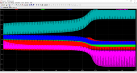
Thanks for the hint, there is some time evolution, but now I see a lot of weird stuff.
E.g. if I use "Skip initial operating point solution" everything settles quite fast, but to a totally different operating point far from reality.
If I leave that box unchecked the evolution is a function of the input amplitude.
Small amplitude, not much happens.
V2 amplitude to 1.6 and the whole thing drifts apart.
I wonder whether I should put any more energy into this simulation or just go back experimenting.
The graphs attached are V2 amplitudes of 1.4 and 1.6.
C1 and C2 are now 10n and R7 is 1000k.
Attachments
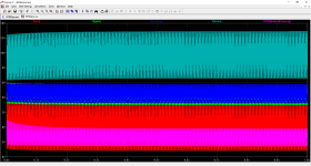
When I replace the FET with a voltage controlled current source in parallel with a constant current source that supplies Idss everything is rock steady.
Dunno whats going on inside that jfet model.
Dunno whats going on inside that jfet model.
Back to the literal drawing board.
I am doing this the first time so I would appreciate if someone looked over my analysis whether I am getting this right and if there is more wisdom to follow.
As I pointed out above I have this circuit to drive my M2 from a DAC output. I guess my M2 maxes out at some 7 to 8V peak-to-peak input voltage. This is what I want to get from this pre-amp stage with a gain slightly above 2. My exact configuration you can see in the spice simulation posted earlier. My feeding voltage Vtot is only 21V.
Currently the preamp clips at output amplitudes of ca 2.4V. So I guess I have to move the load line to get back in business. In the attached graph you find Fig 8 from the data sheet superimposed with my results.
The lines rising with Vds are
Id = beta*(1+lambda*Vds)*(Vgs-VTO)^2
for Vgs = 0 .. -0.5V. The parameters are the first set posted earlier.
The lines falling with Vds are load lines with
Id = (Vtot - Vds) / (Rs + Rb + Rd)
Rs is the source resistor to the ground, R6 in my schematic
Rb is the bias resistor or R4
Rd is the drain resistor R5
The bottom load line in grey is the one from my current configuration: Rd=1000Ohm, Rs=392Ohm, Rb=10Ohm
The solid diamond is where I measure the Q-point via the drop over Rd and Vds. The graph shows that I can't get much more than ca 2.2V in output swing from here, in line with my observation.
I could now try to change the bias resistor to move further down the load line. The open diamonds show top, quiescent and bottom values for a 8Vpp swing. The top value for Id I eyeballed to be 14.2mA, the rest follows from Rd. The load line gives me Vds for the Q-point and
Vgs = sqrt( Id/( beta*(1+lambda*Vds) ) ) + VTO
the bias resistor then becomes
Rb = - Vgs * Id
in this case I find Rb = 17Ohm, Vgs = -173mV, Id = 10.2, Vds = 6.6V
My preferred option is to also change Rd and Rs to move the load line away from treacherously low Vds. The second load line in yellow corresponds to
Rd =800Ohm, Rs=330Ohm, Rb=16Ohm
The Q-point (middle diamond) is at Vgs = -171mV, Id = 10.7mA, Vds = 8.74V.
In understand that with lower Rd I need to travel more Vgs to get the same output swing. To avoid distortion I probably want to stay away from both low Vds and very negative Vgs. Is there a common practice how to place the Q-point for real devices?
For reference I also included the load line (red) from Juma's original circuit. He has the advantage of a total voltage of 24.6V + 4.6V = 29.2V.
So for my next iteration of this little circuit I want to get the best guess I can make. Did I get this right?
Attachments
Typical practice is to choose the net drain resistance (drain load resistor || next stage input impedance) such that the trough of a max amplitude sine wave, requires ~ 80% of adjusted_Idss. In other words, when the input signal commands the JFET to conduct the maximum possible current, that current is comfortably less than adjusted_Idss. (in fact it's 80% of adjusted_Idss). Even in the worst case of maximum signal amplitude you'll never get up to Vgs=zero, you'll always have some safety margin.
And what do I mean by adjusted_Idss ?
adjusted_Idss is the value of Idss which you are 100.000% certain, every single one of your JFETs will exceed. Maybe you plan to pre-test and sort out your JFETs, accepting only those units with Idss>10mA. Then adjusted_Idss=9.5mA.
Maybe you will not or cannot pre-test and sort your JFETs. Maybe you are stuck with whatever probability distribution of Idss, that comes from the manufacturer. Then adusted_Idss = 95% of datasheet minimum Idss.
Be sure to double-check your SPICE models, to verify that modeled Idss is less than or equal to the adjusted_Idss you have decided to abide by.
Obviously you can design your circuits however you see fit, you are not obligated to follow typical practice if you have other ideas.
Thx, it is the "typical practice" I am after - I don't think I have to be smarter than that 🙂
Not for now that is.
Idss is a function of Vds, but I guess we are talking Idss at lowish Vds, b/c looking at the load line this is where the safety margin needs hold.
But I am not sure I fully understood you, b/c it is mostly the bias (in this circuit the choice of Rb) that keeps me away from Vgs=0. Or at least its the combination of bias and slope of the load line (a function of Rd), but not the drain resistance by itself?
Thx for pointing out the input impedance of the following stage. In my case this is 100K, so not an issue, methinks.
One experiment you could try, is to simulate your circuit with whatever input signal that causes maximum amplitude output. Verify that simulated JFET Ids never rises above (0.80 * adjusted_Idss). Never never never. Not even with maximum amplitude AND maximum frequency output. You could put together a .MEASURE directive in LTSPICE and include the MAX function in its operations, to find the maximum Ids in a 310 millisecond simulation window.
If simulated Ids does exceed (0.80 * adjusted_Idss), make whatever design changes you think are wise, and simulate again. Or, pick a different JFET. Or, test and sort your JFETs to a different min-acceptable-Idss threshold.
Another experiment you could try, is to see if your JFET ever operates at frighteningly low VDS. VDS so low that the measured I-V curves are not flat. You could do this with the same maximum amplitude, maximum frequency output signal. But this time your .MEASURE statement looks for the MIN of VDS over a 310 millisecond simulation window.
Last edited:
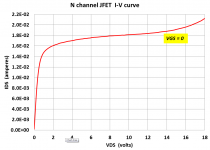
For example, you wouldn't want to operate the attached JFET at VDS < 2.0 volts or so, because that's where its measured I-V curve is not flat. Caution, this is not a BF862! It's just a random NJFET I-V curve that I measured a while ago. I have no idea whether your BF862's curves will stop being flat at 2V, or 1V, or 3V, or somewhere else.
Attachments
Thx. Also for teaching me about the .meas directive. Very handy.
So went back to simulation. The whole contraption is pretty sensitive to the value of R3, the resistor that ties the gate to the bias resistor.
Cycling it from 50k to 500k the gate current (red) has a ball.

With rising values for R3 the gate current develops a dip where the gate voltage has a minimum. At 500k and over the dip tries to go negative, but the simulation clips at zero.
The sim runs for a second, shown here are the last 2ms. For all values of R3 the levels develop in the first 100ms or so.
Gate currents are on the order of 1uA, is this a value that is expected? If not where can I tune the model to remedy this?
So went back to simulation. The whole contraption is pretty sensitive to the value of R3, the resistor that ties the gate to the bias resistor.
Cycling it from 50k to 500k the gate current (red) has a ball.
With rising values for R3 the gate current develops a dip where the gate voltage has a minimum. At 500k and over the dip tries to go negative, but the simulation clips at zero.
The sim runs for a second, shown here are the last 2ms. For all values of R3 the levels develop in the first 100ms or so.
Gate currents are on the order of 1uA, is this a value that is expected? If not where can I tune the model to remedy this?
For example, you wouldn't want to operate the attached JFET at VDS < 2.0 volts or so, because that's where its measured I-V curve is not flat. Caution, this is not a BF862! It's just a random NJFET I-V curve that I measured a while ago. I have no idea whether your BF862's curves will stop being flat at 2V, or 1V, or 3V, or somewhere else.
The transition is usually defined as to where the gate to drain junction pinches off (same Vp as gate to source). So it's easy to keep track of the sum of the voltages and at Vgs = 0 (Idss) the knee is at Vp. The knee points form a parabola.
Scott,
I had added the pinch-off points as dotted line in the pdf posted earlier. The characteristics on the data sheet are quite a bit rounder, though. Unfortunately I find it difficult to measure my own curves. Thats why I am looking how other people would dimension their circuits.
I had added the pinch-off points as dotted line in the pdf posted earlier. The characteristics on the data sheet are quite a bit rounder, though. Unfortunately I find it difficult to measure my own curves. Thats why I am looking how other people would dimension their circuits.
Scott,
I had added the pinch-off points as dotted line in the pdf posted earlier. The characteristics on the data sheet are quite a bit rounder, though. Unfortunately I find it difficult to measure my own curves. Thats why I am looking how other people would dimension their circuits.
There are limitations of the standard model with these short channel devices, unfortunately there are no free simulators (that I know of) that support the higher level JFET models unlike LTSPICE's support of higher level bipolar models.
I have by accident found myself in a position to do something about this but I'm sure it is way down on priorities.
No,.......Idss is a function of Vds,............
Id is a function of Vds, Vgs and temperature.
Idss is a fixed value when Vgs=0, Vds =10V and Tj=25°C
Borbely tells us that min Vds should be >2times Vpinchoff...................
Another experiment you could try, is to see if your JFET ever operates at frighteningly low VDS. VDS so low that the measured I-V curves are not flat. You could do this with the same maximum amplitude, maximum frequency output signal. But this time your .MEASURE statement looks for the MIN of VDS over a 310 millisecond simulation window.
NXP use 8V in their data sheet, but I presume that is not the quantity Mark refers to.Idss is a fixed value when Vgs=0, Vds =10V and Tj=25°C
That's OK, it's a lower voltage device.NXP use 8V in their data sheet, but I presume that is not the quantity Mark refers to.
Do you see that Idss is a fixed value?
Id varies depending on what the circuit asks the device to pass.
BTW, jFETs can operate at much higher than 80% of their Idss.
A B1/DCB1 style Buffer operates the device at 100% of it's Idss for the quiescent state. The AC operatng current takes the device above 100% of Idss.
I regularly use an LTP input stage where quiescent Id is set to 90% of Idss, even though I know that the AC signal will take that close to 100% of Idss.
J.Curl has stated that there is nothing wrong with short term operation at >100% of Idss.
But watch for gate leakage when you do this.
Gate leakage is very dependant on Vds and Tj.
For High Tj and High Vds gate leakage can be 1000 times higher than for conservative operation. Don't go to combined High Vds and High Tj. One or other should be kept low to avoid Ig and the higher one should be respected, not ignored.
Last edited:
- Home
- Amplifiers
- Pass Labs
- BF862 Preamp