I have an RTX-6001 which is really just a very fancy USB stereo ADC/DAC. Not sure what you have, but if you need an upgrade a Motu M2 or M4 might be a good option. I use an M4 for acoustical measurements with an Isemcon mic as well as a couple of standalone MiniDSP USB mics.
At the moment I have a Focusrite Clarett 2Pre I can use for measurement duty. That should be fine. What I don't have is a desk with test gear set up around it where I can assemble, test, measure, etc.
OK, have some progress to report. I managed to come up with a thru-hole layout for a daughtercard on a 25x35 mm footprint PCB. The pins would obviously be the right angle type in practice. This card would plug into a 2+3 holes on the motherboard for signal and power+gnd. It would probably be better if I restricted the motherboard to 8 cards (two sets of four in two lanes) for size purposes, but I will have to see how the cost scales for that layout. A 35mm board mounted to another PCB at a right angle might just fit inside a 1U case... if not I can reduce it by a few mm by moving the pin headers on the daughterboard down, since there are no tracks there.
I want to ask about PS rail decoupling. I used a single 0805 SMD 100nF ceramic cap on the opposite side of the board as the other components so that I could place it directly between the V+ and V- pins of the DIP op-amp package. I am wondering how much bulk capacitance (e.g. 10-100uF local PS reservoir caps) I should place on the motherboard, where, and how many? Just a pair at the entrance to the board, or should I use a smaller value pair adjacent to each daughter-card on the motherboard?
I want to ask about PS rail decoupling. I used a single 0805 SMD 100nF ceramic cap on the opposite side of the board as the other components so that I could place it directly between the V+ and V- pins of the DIP op-amp package. I am wondering how much bulk capacitance (e.g. 10-100uF local PS reservoir caps) I should place on the motherboard, where, and how many? Just a pair at the entrance to the board, or should I use a smaller value pair adjacent to each daughter-card on the motherboard?
Attachments
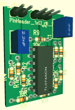

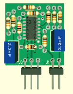
After some investigation of what quad-amplifier op-amps are available in a DIP package and what was not, I decided that an SO package would be better for versatility. After the substitution I was able to redesign the board to be much smaller, now just under 1 inch square. The SO package is really not all that difficult to solder to the pads. After that and the one SMD resistor on the back, everything else is thru hole...
Hmm, I am having trouble creating a decent ground plane on either side. The problem is that the board is quite small and or the components are packed in tightly. There is not enough room in several places for the ground plane to continue through to other parts of the PCB area. I tried to move some tracks and added a via just for ground, but I am worried that this will cause more problems that it is worth. Of course I could oversize the board by 10% and this would open up enough area around the edge of the board for the place to flow to most of the board, but there will still be a couple of islands not covered. Is the ground plane all that important for a line level circuit without much amplification, if any?
I should add that I expect the op-amps will be FET type input state and so resistances will be higher and currents lower.
I should add that I expect the op-amps will be FET type input state and so resistances will be higher and currents lower.
Last edited:
Would be plenty of room for a ground plane, if using SMT resistors, even 1206.
Traces on top to minimize vias, and the ground plane on the bottom.
Traces on top to minimize vias, and the ground plane on the bottom.
Last edited:
No bueno. I tried all SMD and it was (a) a mess and also (b) larger footprint compared to 1/8W thru-hole where you get free access to both sides at each TH. Also, this is a project that will be assembled by DIYers like me who are not well versed in SMD soldering and working with small SMD is a PITA when you cannot read the markings! I am trying to keep it simple with one SO device and one 0805 cap. Hard to mix those up...
Another option to consider is to use a 4-layer board and route power and some traces on the inner layers - in small boards the cost penalty is minimal IMLE. I use JLCPCB out of HK for my boards. The ground plane is helpful. Don't route traces you may want to rework entirely on inner layers at least until the design is completely debugged and settled. Consider capacitance between planes and certain circuit nodes as well, you can window those areas if there is a concern.
I like the OPA164x series and used OPA1644 (quad op-amp) in my SVF filter boards. Other locations are OPA1642 duals.
I like the OPA164x series and used OPA1644 (quad op-amp) in my SVF filter boards. Other locations are OPA1642 duals.
Yes, I'd be surprised if you can't get most all of the traces just on the top layer.
4 layer cost is usually twice that of a 2 layer of the same size, but they're small.
Osh Park charges a total of $10, for three copies of 1 sq. in. 4 layer boards, including shipping.
https://docs.oshpark.com/services/four-layer/
4 layer cost is usually twice that of a 2 layer of the same size, but they're small.
Osh Park charges a total of $10, for three copies of 1 sq. in. 4 layer boards, including shipping.
https://docs.oshpark.com/services/four-layer/
Something of a learning curve, but take a look at KiCad which is open source and very good. Supports up to 32 copper layers. I previously used OrCad (still have a license) and Altium and migrated around 2016 or so.
I'm using Target 3001. I purchased the "light" version a couple of days ago and it has limitations on layers and pads and is for non-commercial use only. I used this software about 8-10 years ago so I am familiar with it and was able to be up and running quickly, producing a fab ready design in only a day starting from a blank sheet. I was considering KiCAD and a couple of other programs but I do not really want to go through the learning process of another design application at this point.
FYI there is a more full-featured and (I believe) free version of Target 3001 but is limited to fab via PCB-Pool/Beta-Layout, which is located in Germany:
https://server.ibfriedrich.com/wiki/ibfwikien/index.php?title=PCB-Pool_Edition
I will be moving there next year, and I can just switch over to that version if I want to create designs with unlimited pins and up to 100 layers.
https://server.ibfriedrich.com/wiki/ibfwikien/index.php?title=PCB-Pool_Edition
I will be moving there next year, and I can just switch over to that version if I want to create designs with unlimited pins and up to 100 layers.
Hello Charlie, if I understand correctly, what you aim to do is build a multiple stage state variable filter for audio purposes? If this is so, why not repurpose a professional 30-band eq? Many I've seen are either analog - and use state variable topology or digital using DSP.
The analog one I use is a Behringer - and it needed some re-work - the original quads were 324 and tl074. The 324s I replaced. It is SMD construction on 4-layer and you could adjust freque cies by changing caps/resistors on board. Surely it's easier than building your own - for a prototype. If you plan on selling, it's another matter.
just my 2 cents on mother/daughter setups - connectors will cause issues. I would make the modules larger such that you use no more than 4 boards max per unit. It also makes the daughterboard easier to secure mechanically...
I think you should invest some time in Kicad... it has its own quirks and limitations, but it is free and quite flexible. I also had access to "the good stuff" at work, but no way would I afford the license... and, little by little, I ended up creating my own libraries (it's lacking in this area too, but parts are easy to create) and chugged away.I'm using Target 3001. I purchased the "light" version a couple of days ago and it has limitations I was considering KiCAD
one of the limitations I run into with kicad is that you cannot have parametric copies of a sub-block... e.g. State variable - you cannot create a block and just change values for each child. You have to copy the schematic, cram it into the page, and then, when ready, do it again all over for stereo. And yep, you get the privilege to arrange the second set of components (for the other channel) anew. But hey... it's free. Apart from that, it's pretty good, and I find myself moving faster than I expected for one-offs.
After 25 yrs using eagle I moved to KiCAD. I had to learn much, but it was worth the effort. A nice feature I got used to is the 3D preview, quite convenient to check component placement. My preferred size with hand-soldering is SMD0805. Just switched to 4-layers to achieve best EM immunity (cell phones!). This is the preview of my latest "guitar strip", i.e. complete pre-amp channel featuring overdrive, reverb, tone control, master volume and soft clipping.
Attachments
- Home
- Design & Build
- Electronic Design
- Best way to incorporate N identical sub-circuits in/on a larger PCB?