DESIGN 2
Appreciate suggestions for improvements.
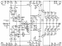
Goal 25watts into 1 ohm for > 100db/w resistive speaker...i.e. 1st watt critical
Design 2
+low noise JFETs in front diff
+high R pull-ups in front diff for good bias point
+over 5ma in VAS
+servo out of signal path
-VAS does not use both differential outputs from front-end diff for gain or CMR
-uses two complementary diffs instead of single stack
Any Suggestions for a better VAS?
Appreciate suggestions for improvements.
Goal 25watts into 1 ohm for > 100db/w resistive speaker...i.e. 1st watt critical
Design 2
+low noise JFETs in front diff
+high R pull-ups in front diff for good bias point
+over 5ma in VAS
+servo out of signal path
-VAS does not use both differential outputs from front-end diff for gain or CMR
-uses two complementary diffs instead of single stack
Any Suggestions for a better VAS?
Attachments
Re: DESIGN 2
Cascode VAS...
LineSource said:Appreciate suggestions for improvements.
...Design 2...
Any Suggestions for a better VAS?
Cascode VAS...
i use orcad 9.2 .I don't know whether my computer has prolems.
My orcad always say " normal vas = cascode vas" .I haven't built cascode differential input stage.
But !fab! Can you try to do it?
Sorry ! My english isn't good!
My orcad always say " normal vas = cascode vas" .I haven't built cascode differential input stage.
But !fab! Can you try to do it?
Sorry ! My english isn't good!
thanh said:i use orcad 9.2 .I don't know whether my computer has prolems.
My orcad always say " normal vas = cascode vas" .I haven't built cascode differential input stage.
But !fab! Can you try to do it?
Sorry ! My english isn't good!
hi Thanh,
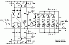
A cascode VAS is a normal VAS with an additional transistor in a cascade arrangement like in this attached amplifier circuit found in the internet. In this circuit, T7 and T9 (T8 and T10 for the negative polarity) forms a cascode VAS. The usual normal VAS is formed by T7 (T8 for the negative polarity). The added cascode T9 with its respective base circuit consisting mainly of D7 and R15 forms the cascode arrangement.
In the last design #2 from Linesource, Q20 and Q21 could be replaced by a cascode VAS in the same manner.
The main benefit of cascode is a much larger frequency bandwith. The cascode transistor should be polarized with the lowest "working" base voltage. In the attached circuit, it means D7 (and D8) with values of about 4 volts or so depending of voltage across R17 (R18).
For the differential input, I like the cascode arrangement also. See the following thread (post # 22) for my personal preference: http://www.diyaudio.com/forums/showthread.php?postid=395669#post395669
In the last design #2 from Linesource, the cascode principle is already there (adapted for jfet) in the diff input stage.
Fab
fab! my orcad say that there is not difference about bandwidth of normal vas and cascode vas.
Can you understand me?
sorry to my bad english!
Can you understand me?
sorry to my bad english!
How are you simulating the VAS?
If you are simulating the VAS by itself, and driving it with a voltage source, you won't see any difference, because the bandwidth enhancement of the cascode comes from its effective reduction of the capacitive loading of the previous stage.
If you are simulating the entire amplifier, then maybe there is another factor limiting the bandwidth at a lower frequency than the VAS limits it.
-- mirlo
fab! your post 245
what is the function of R22.....R29?
do i need these if i use BJT instead of MOSFET?
what is the function of R22.....R29?
do i need these if i use BJT instead of MOSFET?
Hi Thanh,
You are very curious. I have some difficulty to catch up to respond to all your questions. However, I am glad that you are interested!
1) for "what is the function of R22.....R29?
do i need these if i use BJT instead of MOSFET?"
Gate resistors for mosfet are almost imperative to avoid high frequency oscillation. For BJT, this is not a real concern. However, even though I have not designed a lot with output BJT (I like too much the mosfet) I would say that base resistors would not hurt. Some designs have them but some not. Maybe someone here can comment on the real benefit of base resistors in output BJT (limit base current in overload conditions?)?
2) For "So can a cascode input stage increase the bandwidth"
Yes, but read carefully the comments from the others. As pointed out, the bandwith can be increased as long as the other components (mosfet input capacitance, loading of previous stage, etc.) do not reduce the effect of the cascode on bandwith.
Fab
linesource..does your second dedign have a buffer stage between the VAS and input?...what is the advantage of this...and how do you calculate the component values?...thanks for any input
This amp will be in the same chassis as a digital crossover and D/A converter and share the same +/- 15V supply. The 10K input impedance was selected because it is lowest gate resistance that can deliver the noise floor on the J2SA389. The gain in each differental stage is 2000 / (100 + 8=Rfet) = 18.5, and each leg of the diff runs 3ma. The VAS stage runs 5.5ma through low noise BJTs with hfe of 350-400 that only have to drive 100-200uA into the current source regulated Class A bias-buffer. In addition to reducing the distortion with a factor of 5-10 times, this bias-buffer allows the use of low noise small signal transistors in the voltage amplifier. The voltage swing is also increased, since the transistors are placed in opposite direction, and are using current generators with a current of 30-40 mA. One can lower these current generators to limit maximum output current for speaker protection. There is no voltage amplification in the output stage, but the current amplification is very high. R23 and R24 can be used to limit gain, and C3 and C4 can be used to limited slew rate and maximum frequency. The DC servo is outside of the signal feedback loop, and can only provide modest compensation by slightly tugging on the well filtered current source diodes.
Driving a >100db/watt, 1 ohm ribbon is a good challenge for any amplifier designer as it combines the low noise demands of a preamp with brute Class A output current, and I hope more circuits and analysis are added to this thread.
Driving a >100db/watt, 1 ohm ribbon is a good challenge for any amplifier designer as it combines the low noise demands of a preamp with brute Class A output current, and I hope more circuits and analysis are added to this thread.
linsource! what simulation sofware are you using?
how is the 2nd 3rd harmonics of your circuit at post 241 if output voltage is 25V?
how is the 2nd 3rd harmonics of your circuit at post 241 if output voltage is 25V?
Thanh,
I have not built this amplifier yet, as I am still waiting for parts. The transistor Spice models I have from vendor sites are not detailed enough to make useful simulations of harmonic distortion.
If anyone has detailed Spice models for these transistors, please post.
J2SK389 BL and V
J2SK170 BL and V
JSJ109 BL and V
J2SJ74 BL and V
QBD140
QBC139
Q2SC2240
Q2SQ970
QMJL3281a
QMJL1302a
2SC2922 standard and P or G grade
2SA1216 standard and P or G grade
Driving a >100db/watt, 1 ohm ribbon is a good challenge for any amplifier designer as it combines the low noise demands of a preamp with brute Class A output current, and I hope more circuits and analysis are added to this thread.
LineSource said:This amp will be in the same chassis as a digital crossover and D/A converter and share the same +/- 15V supply. The 10K input impedance was selected because it is lowest gate resistance that can deliver the noise floor on the J2SA389.
LineSource,
You still have some serious misunderstandings of low noise design principles evident in the front end and your comments
Forget noise figure/factor it simply doesn’t apply for what you are doing, calculate the total equivalent input noise voltage to compare designs, a 3-5 dB “bad” noise figure with a sub 100 Ohm source is much quieter than a “good” 0.5 dB noise figure with a 10 KOhm source – and you have told us you have a low Z source direct from the DAC output filter/buffer op amp, adding series R never improves total noise
Your schematic doesn’t have a 10 K source Z, the input signal voltage source shorts it out –but your feedback network does have a high R which increases noise and distortion with the (potentially) low noise fet front end, the feedback network R at the negative input should be low and ~= the positive input source R
The biasing in schematic #2 is more likely to work but the single sided output from each diff pair puts tail current source noise back into the equation – you need higher ref V (probably RC filtered) to allow a higher current setting R to reduce tail current source noise contribution – also consider whether the added pfet diff pair actually reduces noise, it won’t if pfet en > 1.7x nfet en (assuming gm, Rd adjustment for = contribution to the amplifier’s total gain)
Of course you can ignore most of this with little effect on the result in your application because you don’t actually need an ultra low noise amp in the first place – the best monolithic DAC chips barely manage 120dB (+ 2, or 3 or a little more if you start paralleling DACs)
The DAC S/N are typically speced with A weighting re >=2 Vrms outputs – simplifying by using the more conservative assumption of unweighted white noise;
2 uVrms/sqrt(20KHz) ~= 14 nV/sqrt(Hz) spot noise
adding 1/3 of this as your amp’s input noise only adds 1 dB to the total which means <4 nV/sqrt(Hz) gives an imperceptible noise increase – if you stick your ear on the speaker to get above the typical +20 dB “really quiet” room noise
pursuing any one parameter to its max (or min) in engineering usually leads to tradeoffs elsewhere, I believe it has already been pointed out that large area low noise fets have increased nonlinear junction capacitances that increase input stage distortion, operating at high currents for low noise also increases thermal modulation errors (that aren’t dynamically modeled in Spice at all)
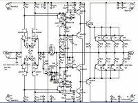
UPDATE STACKED COMPLEMENTARY TOPO
Here is an update of the stacked complementary topology which uses unequal pull-up resistors in the differentials to allows 10ma bias for the cascode VAS, high gain for the input and low gain for the feedback.
It also lowers input and feedback R as recommended by jcx.
Here is an update of the stacked complementary topology which uses unequal pull-up resistors in the differentials to allows 10ma bias for the cascode VAS, high gain for the input and low gain for the feedback.
It also lowers input and feedback R as recommended by jcx.
Attachments
Hi linsource! I have tried to add some new component in orcad but it is unsuccessful! I remark that this depend on your sofware which you are using.
2sk170www.diyaudio.com/forums/showthread/t-1977.html
www.diyaudio.com/forums/showthread/t-4797.html
www.high-end-online.de/2SK170.mod
Do you live at silicon valey? Are there many companys made transistor there?
2sk170www.diyaudio.com/forums/showthread/t-1977.html
www.diyaudio.com/forums/showthread/t-4797.html
www.high-end-online.de/2SK170.mod
Do you live at silicon valey? Are there many companys made transistor there?
- Status
- Not open for further replies.
- Home
- Amplifiers
- Solid State
- best topo for 25W class A into 1 ohm resistive load?