
I'm teaching myself how to make PC boards, first try is a 12B4 (single triode) simple grounded cathode circuit.
On the 12B4 pins 2 and 7 are both internally connected to the grid. Pin 7 looks like the better candidate for the stopper resistor and connection to the input signal because the engineers left pins 6 and 8 unused, nice. So I was going to have pin 2 then be unused and just soldered to a pad that goes nowhere. Pin 2 sits right between the filament center and and the cathode, and pin 7 has roomy-ness that was my reasoning to use pin 7 for the whole input network stopper, leak, pot and jack.
So my question is... Is it ok you think to leave pin 2 hanging since 2 and 7 are connected and I'll have a stopper on pin 7? Or should I run a trace from 2 to 7 on the PCB as well? Would not running another trace from 2 to 7 just be creating a bigger "antenna" on the whole grid? Perplexed.
Last edited:
I have a different answer, according to the application.
This tube was designed to drive a TV Vertical CRT yoke.
You are going to use it to amplify audio frequencies, Right?
Are you planing to be drawing Lots of grid current?
Then connect pins 2 and pin 7 together.
Not planing to draw lots of grid current, then leave pin 2 unconnected.
Or, are you going to use it as a Series Regulator tube?
Will you draw Lots of grid current?
Then connect pin 2 and pin 7 together.
Or, are you going to use it to amplify RF frequencies at several Mega Hertz?
Connect both pin 2 and pin 7 together to lower the effect of inductance for Mega Hertz.
I have used a 6C45pi tube that has 2 grid pins. The application was as an audio amplifier. I only ever connected one grid pin. Because of the tendency of the tube to oscillate, I used 1 grid stopper, and connected it only to one grid pin. The other grid pin was not connected to the circuit.
Just my opinions.
Last edited:
Thanks 6a3 and euro,
It is a pre Amp stage. Another alternative I just thought of this morning is to not even make solder pads for pins 6 and 8 and just clip the socket pins. I could do the same for pin 2, no solder pad at all and clip the socket pin off. That would leave pin 2 with the shortest "antenna" that is possible to construct here. And it would leave pin 7 with a whole lot of space away from inducted hum. 6a3summer I was wondering why this tube had two grid pins at all, it was a video or vertical amp!
It is a pre Amp stage. Another alternative I just thought of this morning is to not even make solder pads for pins 6 and 8 and just clip the socket pins. I could do the same for pin 2, no solder pad at all and clip the socket pin off. That would leave pin 2 with the shortest "antenna" that is possible to construct here. And it would leave pin 7 with a whole lot of space away from inducted hum. 6a3summer I was wondering why this tube had two grid pins at all, it was a video or vertical amp!
6A3 said it well.
The grid itself is a piece of metal. It'll have quite low resistance. So at low frequencies (think audio) there's no impact of leaving one end or the other disconnected.
Tom
The grid itself is a piece of metal. It'll have quite low resistance. So at low frequencies (think audio) there's no impact of leaving one end or the other disconnected.
Tom
1. If you remove some pins from the socket, you will reduce the physical strength of the socket to hold itself and to hold the tube in place.
That might change how microphonic the tube is in its environment.
If having pin 2 and a copper pad on the PCB causes pickup of RF or other signals (such as the clock frequency from a 128kHz oversample digital player), then you have some real serious problems.
Just removing pin 2 on the socket and the copper pad will not fix that.
I had a job in the shipyards, inside of a screen room. The job was to measure sub-microvolt sensitivity of US Naval RF Receivers.
As good as the screen room was, with highly conductive finger-stock on the doors, and also some special power mains filters, you could not test the receiver sensitivity when the welders in the shipyard were working. Too much of that came through the power mains filters, as near perfect, and as expensive as the filters were.
I also had experience in a spectrum analyzer engineering group, and we had special shielding techniques, ground loop reduction, etc.
2. I think the engineer who designed the 12B4A and 12B4B is dead. We can not ask him why he used 2 grid pins.
I used to want to talk to the design engineer of the WE 300B. But of course, Charles Whitener reminded me that he was dead.
tomchr,
About 50 years ago I was in Calgary during college spring break. (Cold!)
We went to a college auditorium there, and heard the most glorious Brass Ensemble
playing classical music. I will never forget that.
When we listen to our Hi Fi playback systems, we should listen and enjoy.
But that is nothing compared to live music.
6a3 clipping socket leads is something I could try and still have the option of soldering for other tries. So ill make pads for 2; 6 and 8, but I don't necessarily have to solder socket pins to them. Id have the option of clipping them or not. As for pad 2 ill try to work in pads for an optional grid stopper there. Ill probably have 10 copies of the PCB made so I can then try all options if I have issues. My goal is just to learn PCB making by making a collection of small boards with standard topologies grounded cathode, cathode follower, differential, etc. For experimenting, no part values silkscreened, just the function of each part silkscreened, stopper, leak; bleeder, coupling cap, plate resistor, cathode resistor, bypass cap, decoupler, etc. Each board would accommodate a different standard tube basing diagram. Having these will let me strap together standard modules quickly I just find the board for what base socket base id I want and what topology I want, then solder on the part values I want. Kind of like a learning lab using a library of small empty pcb cards by tube base and circuit type.
Last edited:
If you clip the socket pin, it might intermittently contact the pad. That might cause
some interference, off and on.
If you Pull Out the socket pin completely, it can not intermittently contact the pad.
Soldering, removing, and re-installing and re-soldering a tube socket a number of times can lift pads, remove through hole plating, etc.
Let's worry about the outer layer of the onion, before we design a special PCB that will remove the most inner layers of the onion.
I think you are still worried that leaving pin 2 un-connected will not work in your circuit.
A simple hole in the PCB, with no pad (#2 pin) is another alternative, using a complete
unmodified tube socket.
If you want to make several versions of PCB, and mount different modified or un-modified sockets on each one, seems to be a reasonable experiment.
Just remember that trying different PCBs will require soldering and unsoldering the pads that connect to the external wiring that goes to the PCB.
Making a universal PCB for 9 Pin Noval sockets may work for certain tubes, but may not work for a 400MHz 9 pin tube.
Last edited:
About a decade ago I built a preamp with 12B4a.
GE tubes, CLCRC smoothing, resistor loading, grid stopper on only one grid pin.
It oscillates like mad, even at 10k...100R range of grid stopper.
When I used 1k grid stopper on both grid pins, the oscillation stopped.
I like the tone of 12B4a, but due to my limited stock (each GE), using its as line preamp the microphony was confusing.
About a decade ago I built a preamp with 12B4a.
GE tubes, CLCRC smoothing, resistor loading, grid stopper on only one grid pin.
It oscillates like mad, even at 10k...100R range of grid stopper.
When I used 1k grid stopper on both grid pins, the oscillation stopped.
I like the tone of 12B4a, but due to my limited stock (each GE), using its as line preamp the microphony was confusing.
Due to variables like this I added pads and jumper pads to allow someone to wire it up any number of ways. Two stoppers, pins 2 and 7 connected with one stopper, pin 2 floating, etc. It will be versitile in this way.
When I get a layout done ill repost it to this thread. Almost done I just need to check and double check it all.
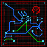
First draft of my PCB
Here is what I've done... J1 can be used if you only want one grid stopper on both pins 2 and 7 connected. J2 can be used if you want two independent grid stoppers. Or no jumper used if you want pin 2 to just float, or you want to clip off the pin 2 socket pin.
The board is exactly 3 x 3 inches, I'm leaving the full ground plane on both sides so that it will be real "stiff" for inserting the tube with no flex. All the parts are on the blue trace side of the board, with the exception of the tube socket which is on the green trace side. The only traces I sent to the green trace side is the B+ run. Note there are no part values, just part functions silkscreened, the user just needs a simple grounded cathode circuit he picks the part values. Note there are 4 terminal blocks in, out, B+/gnd, and the filament. I put the filament block right close to the tube so you can come in with a twisted pair right up to the tube. There is one star ground and that is a through hole that also attaches to both ground planes on both sides. All other pads are through hole. All traces have a wide gap from the ground plane. The traces in the grid circuit are narrower so as to not make bigger antennas.
I'm really liking PCB boards now, I never really accepted them before, as long as the tube is on one side and the parts on the other side they can go into chassis easily.
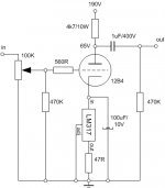
The board is based on the schematic shown, with the only difference being that I added an elco decoupling cap right at the B+ terminal.
Since this is my first PCB attempt I'm all ears to criticism.
Here is what I've done... J1 can be used if you only want one grid stopper on both pins 2 and 7 connected. J2 can be used if you want two independent grid stoppers. Or no jumper used if you want pin 2 to just float, or you want to clip off the pin 2 socket pin.
The board is exactly 3 x 3 inches, I'm leaving the full ground plane on both sides so that it will be real "stiff" for inserting the tube with no flex. All the parts are on the blue trace side of the board, with the exception of the tube socket which is on the green trace side. The only traces I sent to the green trace side is the B+ run. Note there are no part values, just part functions silkscreened, the user just needs a simple grounded cathode circuit he picks the part values. Note there are 4 terminal blocks in, out, B+/gnd, and the filament. I put the filament block right close to the tube so you can come in with a twisted pair right up to the tube. There is one star ground and that is a through hole that also attaches to both ground planes on both sides. All other pads are through hole. All traces have a wide gap from the ground plane. The traces in the grid circuit are narrower so as to not make bigger antennas.
I'm really liking PCB boards now, I never really accepted them before, as long as the tube is on one side and the parts on the other side they can go into chassis easily.
The board is based on the schematic shown, with the only difference being that I added an elco decoupling cap right at the B+ terminal.
Since this is my first PCB attempt I'm all ears to criticism.
Attachments
Make it a stereo board to avoid excess wiring and way easier build, use standard Phoenix MKDSN style connector blocks for B+, use Molex KK/JST style 2.54 mm input/output connectors, use larger footprint (higher voltage rated like 100V) caps for cathode bypass, use 2 grid stoppers so at both pins also in way higher value like 3k3 for 12B4a as they will oscillate otherwise for sure, use an RC input filter with - 3dB point at 70 kHz, include pads for a CCS (based on 10M45), use higher value output caps like 3.3 µF or 4.7 µF, use 100 Ohm output series resistors, add muting relay shorting outputs to GND with 20 seconds delay because of sometimes strange sounds 12B4a can make during warm up, include PSU so essentially a 1 board system, get rid of the LM317 and just use a resistor, include footprint for Alps style volume control and add extra pads just in case you will use another form of volume control, use a semiconductor regulator for B+ for true silent operation.
Last edited:
euro21,
Was your 12B4A cathode bypassed with a capacitor to ground?
What was the 12B4A plate load?
Resistor?
Did the output connect to a long shielded cable?
What was the input circuit?
Was your 12B4A cathode bypassed with a capacitor to ground?
What was the 12B4A plate load?
Resistor?
Did the output connect to a long shielded cable?
What was the input circuit?
Make it a stereo board to avoid excess wiring and way easier build, use standard Phoenix MKDSN style connector blocks for B+, use Molex KK/JST style 2.54 mm input/output connectors, use larger footprint (higher voltage rated like 100V) caps for cathode bypass, use 2 grid stoppers so at both pins also in way higher value like 3k3 for 12B4a as they will oscillate otherwise for sure, use an RC input filter with - 3dB point at 70 kHz, include pads for a CCS (based on 10M45), use higher value output caps like 3.3 µF or 4.7 µF, use 100 Ohm output series resistors, add muting relay shorting outputs to GND with 20 seconds delay because of sometimes strange sounds 12B4a can make during warm up, include PSU so essentially a 1 board system, get rid of the LM317 and just use a resistor, include footprint for Alps style volume control and add extra pads just in case you will use another form of volume control, use a semiconductor regulator for B+ for true silent operation.
A lot here and thanks, first off I am making these a little leaning boards not as a final project, so no need for stereo. Its my education. I'd like to make all the basic circuit topologies like grounded cathode, cathode follower, differential, even grounded plate and grounded grid, etc. all with a selection of maybe five or six different standard tube bases. as small modules I can strap together fast. I just started with a 9AG base this time because its a single triode and I happen to be reading about the 12B4 here lately. As for part values those would be determined based on whatever tube a person chooses to experiment with, and the operating points they want to experiment with. As for CCS vs resistors I just made space for large resistors and the user would make a CCS "shield" with the same footprint dimension to learn the difference in a resistor vs a CCS. I'll probably design thoseCCS "shield boards" as part of this whole exercise. So they just solder on a CCS shield much like they do with Arduino shields. I wasn't going to put pots or jacks on the boards because that limits how you can use the board in a chassis. All power just comes into the boards from a persons bench supply or a supply they built.
Some of the suggestions are appropriate, I should add some pads for a muting switch and even a power switch. And I will footprint the cathode bypass bigger for larger voltage cap there as you mentioned.
The whole idea for these is basically "breadboarding" with PCB modules.
Thanks
oh boy it turns out that there is only one tube in existence that uses a 9AG base and that is the 12B4. I was thinking there would be at least a few 9AG tubes. So this board is single-purpose tube. I'll have to find a base that is more widely used for my next layout.
first off I am making these a little leaning boards not as a final project, so no need for stereo. Its my education.
I don't understand anything of this?! You will test and listen stereo (at least). It is exactly right for your education to make the design as optimal as possible in all aspects. Using mono channels is not making things easier (except on the PCB drawing board). If the idea is breadboarding with PCBs then it would exactly be the right thing to add all extra PCB pads on 1 PCB. This for safety and for easy modifications/testing. The use of PCB connectors is almost mandatory in the day and age and these are the typical PCB blocks not chassis mount connectors which are indeed difficult when one is not that experienced (yet). Soldering wires directly to boards is plain old fashioned and unsafe.
The 12B4a is a very good tube for todays sources and todays impedances. Even if it were a single purpose board then the tube would still be the right guy for the job and you would still have to buy tube sockets (also if you make the same mistake as many others to adapt to high mu tubes). Except when using old phono stuff one often does not need gain in 2020 which makes many many well known tubes way less interesting to experiment with. So the logic and the reasoning are a little flawed IMO (a muting switch?) but have fun with the project. Remember that there is a chance to do things right at once and that a well designed device might be of real use in the real world.
The project is typical what I see on the tube world. One wants to do something and of course there must be a tube in it. Normally one starts to define what is needed. This is why many designs are not well fit for the purpose where they are used for and why many devices are superfluous. Like adding an extra high gain device after the sources 2Veff output to the amplifier!?!? The experiments nearly always end up being reused and then again a device that is built as a pastime ends up being not 100% fit for the job.
Last edited:
This exercise is to learn how to make some simple PC boards through the whole process of gerber then ordering it, learning how to talk to the PC board mfg without failing the giggle test, etc. And to learn the basic building block circuits better, starting with the grounded cathode circuit of course.
Having a supply of throw away PC boards for that circuit set up for maybe 5 different tube bases will let me try out a lot of different tubes, experiment and not have to constantly clear off my bench and lose old experiments. I can just go get the board I made before and resume.
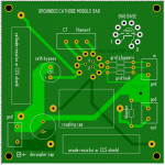
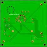
Here is where I'm at currently with this board. I will repeat this exercise with the 6Q tube base next as that will give me a testing board for 6J5, 6C5 and many other single triodes. I wish I had picked that first because the 9AG base only supports one tube, the 12B4.
Having a supply of throw away PC boards for that circuit set up for maybe 5 different tube bases will let me try out a lot of different tubes, experiment and not have to constantly clear off my bench and lose old experiments. I can just go get the board I made before and resume.
Here is where I'm at currently with this board. I will repeat this exercise with the 6Q tube base next as that will give me a testing board for 6J5, 6C5 and many other single triodes. I wish I had picked that first because the 9AG base only supports one tube, the 12B4.
Attachments
Please try to exercise designing a device for a certain purpose in real life situations and for actual use. Throw away projects are not the idea of being green. You can forget using any high gain tube when the device will be used with "modern" (younger than 40 years) sources as you will lose time and be busy with a hampered device from the start otherwise. The idea to choose a certain tube and then find a use for it in a design is plain wrong design technique but it seems standard in the tube DIY world. No one has 5 different car engines and starts building throw away cars for the engines that are in the barn.
You have chosen a very good candidate for todays demands as it has low gain and can drive solid state power amplifiers with relatively low input impedances. Make the device versatile so it can be combined with all normal stuff before it and with all normal stuff behind it and make sure power on/off sequence is of no concern. That is a challenge!
You have chosen a very good candidate for todays demands as it has low gain and can drive solid state power amplifiers with relatively low input impedances. Make the device versatile so it can be combined with all normal stuff before it and with all normal stuff behind it and make sure power on/off sequence is of no concern. That is a challenge!
Last edited:
Please try to exercise designing a device for a certain purpose in real life situations and for actual use. Throw away projects are not the idea of being green....
Points taken. I'm not ready yet to fully design and make something that is good enough to use in my system, and proven kit assembly isn't something fun for me I've made many kits. So its baby steps for me, assemble a small circuit and see how it works, then come back to it. By throwaway I meant just a series of experiments, not garbage. I'm guess looking for a learning methodology similar to the Arduino community, small boards, shields, experiments, which eventually lead to making a showcase Amp.
- Home
- Amplifiers
- Tubes / Valves
- Best grid traces for 12B4 PCB