You're welcome 🙂
Raising the 5 volts even a little could be worthwhile. You will have to experiment.
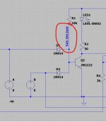
Also you can see the difference the choice of diode makes. If you run the sim with the Schottky devices and with A and B at zero volts then you have just 100mv on the base of the first transistor which ensures it is fully off.
Use ordinary diodes and it all becomes to marginal and you can not guarantee the transistor will be fully off under all conditions.
Raising the 5 volts even a little could be worthwhile. You will have to experiment.
Also you can see the difference the choice of diode makes. If you run the sim with the Schottky devices and with A and B at zero volts then you have just 100mv on the base of the first transistor which ensures it is fully off.
Use ordinary diodes and it all becomes to marginal and you can not guarantee the transistor will be fully off under all conditions.
Attachments
I couldn't ask for more! Thanks a lot Mooly!
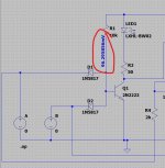
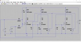
Complete schematic for this is a pain to draw. See attachment for a simplified version. Logic level ~3V. Vcc is not written in stone. Can be anything convenient.
Why do you show this?
It is COMPLETELY unrelated to your earlier post.
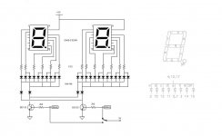
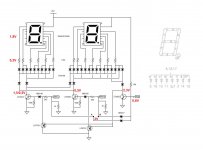
It supposed to show the basic blocks of my circuit to give you an idea about the load. These combined with the logic gate circuit that Mooly kindly developed hopefully will make a four digits, eight commands digital display. I'm about to finalize the pcb. I'll share results.
Remember this? Eventually I built a prototype! Unfortunately is partially working... I repost the schematics for your convenience. The load is LED digits with individual resistors per segment and two stages of diodes after that. The current varies from 100mA to more than 250mA depended on the number displayed. I thought to use BD135 to withstand this load. When only "A" or "B" is on it works a charm! But for "A+B" -the AND gate- it doesn't switch off "A" and "B" unless the voltage at Q1 collector is 250mV and less i.e. increasing the load resistors or decreasing Vcc but then the LEDs fade out. To keep the current per segment at 10mA the collector sits at 600mV and the PNP transistor -I used BC560 with 1k base resistor- doesn't work. Do you have any suggestions? Seems to be so close to make it work...
Attachments
> to more than 250mA .... But for "A+B" -the AND gate- it doesn't switch off "A" and "B"
3V logic, 2.2k base resistor. You have just over 1mA base current. Times Beta of 100, this will support 100mA load current. Beta may be larger? But ON/off applications should be totally overdriven, not marginal.
Can you make more base current? If not with your present CPU, maybe with a 9V battery just to try?
Yes, I thought of that too but I tried it before I tweak the load resistors and while using BD136 instead of BC560. Logic 3V is suitable to drive directly LEDs at 8mA or less according specifications. I'll try again.
EDIT: However I think something has to do around Q1?
EDIT: However I think something has to do around Q1?
Last edited:
I assume low Vgs is for the P-channel? How about this one? http://ww1.microchip.com/downloads/...-Mode-Lateral-MOSFET-Data-Sheet-20005447A.pdf And something like this for the N-channel? https://docs.rs-online.com/7f51/0900766b80d2467b.pdf
The P channel FET is a lateral... not seen these before. These have a very low turn on voltage which is what you want. The other one is no good as it has a pretty standard 4 volt threshold.
Lots of options, thanks! What should be the requirements for Darlingtons? I don't seem to find my way with transistors... Regarding those N-channel mosfets I find this https://gr.mouser.com/datasheet/2/268/TN0702%20C080813-965109.pdf for Vgs<1V-Id=530mA and this https://gr.mouser.com/datasheet/2/115/ZVN4310A-92835.pdf for Vgs<3V-Id=900mA. Are these Id to be trusted for TO92 package? This one seems ideal https://gr.mouser.com/datasheet/2/427/sihld110-1768753.pdf however rejected solely from the looks of it...
The last one of those would possibly work. What you look for is the Vgs vs Id value, the transfer characteristic. You want lots of drain current for low values of Vgs. The lateral FET from earlier does that easily.
High values of Id (or Ic for transistors) in a TO92 package is fine, Remember the transistor dissipates little power when fully on (no voltage across it) and so the current can be high.
The maximum power dissipation of a T092 package will always be low of course. It is up to the designer to make sure that the current flowing through and the voltage across the device do not exceed that power rating.
Also remember you don't have to use all FET's or Darlingtons in the design. You can use one where needed and keep the other transistors as they are.
Attachments

So, I'm thinking to try the lateral FET with BD135, it might work marginally. Plan B is this https://www.diodes.com/assets/Datasheets/ZTX652.pdf for the AND gate driver or am I wrong once again?
Those are just NPN's, not FET's.
They are quite high gain according to the data sheet so could be worth a try I suppose.
They are quite high gain according to the data sheet so could be worth a try I suppose.
Reading from the left, the first transistor will follow the base voltage on the emitter. The other two will just be on or off, depending on the bias point. The problem is that current flows via the load resistor and through the B-E junction of the PNP device straight into the NPN B-E junction.
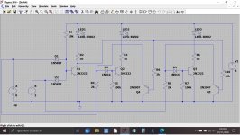
Apologies for the prolonged silence but I was waiting for new parts and overseas shipping takes longer these days. So I tried the LP0701 P-channel lateral FET mentioned above with ZTX653 for the NPN drivers and unfortunately doesn't seem to work either... Even tried BC547 in this position with no luck and surprisingly without a lost part given the bench psu was reading 260mA. It makes me think that the AND gate driver does not take the current for some reason...And the collector voltage stays at ~ 0,6V no matter what.
No problem 🙂 but you will have to remind me exactly which circuit version you are using.
Next step would be to measure and record all the circuit voltages in each possible input state and try and see where it is not working.
Once we have the exact circuit you can take a screen shot of it and enter your voltages in... then we can try and make sense of it and see where it is different to the simulated version.
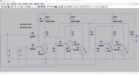
Thank you! Honestly, the reason I don't give up this is because of your efforts!🙂 Schematic can get insane easily. I drew one which is representative of the real circuit. Gate "A" lights number 48 and "B" lights number 96. I made the AND gate to light number 1 for clarity. In real life there are four digits for eight numbers.😱 That is 100 diodes... Six of the numbers are driven from straightforward drivers and then I use two AND gates to combine two pairs of them to drive the last two numbers. Individually, each driver seems to work nice. But the AND gates seem to introduce some disturbance. I measured voltage on the circuit. The LEDs take 1,8V. Although I would like to keep them at 10mA, they feel better at ~ 6mA. That is 0,3V across the load resistors. Then there are two layers of diodes dropping ~ 1,4V. Then, when only "A" (or "B") is on, their driver collectors sit at 1,5V from ground. But when "A+B" is on -the AND gate- this drops to 0,5V and the collector of the AND gate stays at 2,3V. I forgot to say that I used a combination of your suggestions i.e. NPN ZTX653 for the drivers and P-channel FETs for the "switches".
EDIT: Schematic is indeed a nightmare... The AND gate as drawn does not light number 1 but something like _|
Six of the numbers are driven from straightforward drivers and then I use two AND gates to combine two pairs of them to drive the last two numbers. Individually, each driver seems to work nice. But the AND gates seem to introduce some disturbance. I measured voltage on the circuit. The LEDs take 1,8V. Although I would like to keep them at 10mA, they feel better at ~ 6mA. That is 0,3V across the load resistors. Then there are two layers of diodes dropping ~ 1,4V. Then, when only "A" (or "B") is on, their driver collectors sit at 1,5V from ground. But when "A+B" is on -the AND gate- this drops to 0,5V and the collector of the AND gate stays at 2,3V. I forgot to say that I used a combination of your suggestions i.e. NPN ZTX653 for the drivers and P-channel FETs for the "switches".EDIT: Schematic is indeed a nightmare... The AND gate as drawn does not light number 1 but something like _|
Attachments
Last edited:
- Home
- General Interest
- Everything Else
- Basics on transistor drivers