I am messing around with the Crystal CS8412 digital reciever chip, trying to build a decent SPDIF input stage for it and realizes this task is not as trivial as it first appeared to me...
After reading through an informative thread on the subject, I could not help myself from stopping again and again reading through WMS's post at http://www.diyaudio.com/forums/showthread.php?postid=27860#post27860. This definitly looks like the way to go, and the 6111 triode idea melted me.... My bet will, I think, be to use the 74HC86 (or VHC) wired as a phase splitter for the digital signal, using a 6111 dual triode pencil tube to amplify both phases into an Aes-EBU transformer...
Now, when using the 6111 tube in place of transistors as WMS suggests, I would have to set it up as cathode follower with coupling capacitors wouldn't I?
Also, Partsconnexion has a Aes-EBU-tranny that might be a good alternate to the Lundahl LL1566 I have, since it appears (judging by it's picture, i have to check this) to have centertap on its primary, wich might be beneficial to connect to ground reference in a balanced scheme?
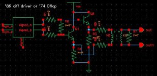
Could anyone help me get somewhere with this? Any thoughts or ideas? Here is a copy of the circuit MWP suggests, but using transistors...:
After reading through an informative thread on the subject, I could not help myself from stopping again and again reading through WMS's post at http://www.diyaudio.com/forums/showthread.php?postid=27860#post27860. This definitly looks like the way to go, and the 6111 triode idea melted me....
My bet will, I think, be to use the 74HC86 (or VHC) wired as a phase splitter for the digital signal, using a 6111 dual triode pencil tube to amplify both phases into an Aes-EBU transformer...Now, when using the 6111 tube in place of transistors as WMS suggests, I would have to set it up as cathode follower with coupling capacitors wouldn't I?
Also, Partsconnexion has a Aes-EBU-tranny that might be a good alternate to the Lundahl LL1566 I have, since it appears (judging by it's picture, i have to check this) to have centertap on its primary, wich might be beneficial to connect to ground reference in a balanced scheme?
Could anyone help me get somewhere with this? Any thoughts or ideas? Here is a copy of the circuit MWP suggests, but using transistors...:
Attachments
Why do you think that you need to amplify it? The output is supposed to be 0.5 V p-p, not 50 V p-p.
Jocko
Jocko
Jocko Homo said:Why do you think that you need to amplify it? The output is supposed to be 0.5 V p-p, not 50 V p-p.
Jocko
True, but the output of the 74HC86 OR-gate is hardly 0.5V p-p is it? I'm not an expert on this digital stuff but I had the impression it was much lower.. Are you saying a 74xx86 chip can drive the tranny on it's own? and wouldn't the signal benefit from a buffer (with regards to reflections, etc) even if the buffer provides only minimal gain?
Edit: Also, the CS8412 chip will have no problems handling a higher, say 3V p-p signal (example out of the blue), with it's self-biasing feature?
Apparently, Harry have had good experiences using the '86, so I thought it was a somewhat safe and way easier approach than reclocked flipflop or other suggestions i've seen.. Here's what he says;
HarryHaller said:I have used the 74HC86 as a phase inverter for driving balanced digital out for AES/EBU interfaces. It works real well. Jocko said this circuit was too good to give away for free!
Uh..........the output is CMOS level..............5 V p-p. You need to reduce it, not amplify it.
As for reclocking F-F..........put it in front of the '86, and only use one ouput. Yeah, too good to give away for free, but what the hey............
Don't use the Lundahl. They make good audio transformers, but SPDIF onrs are totally different. I would not use them. Or any designed for AES-SPDIF conversion. Or 2:1 ones, either.
Jocko
Thanks for your reply, Jocko.
Edit: PE-65612 pdf @ http://www.elfa.se/pdf/56/05655055.pdf
edit: edit: BTW they are pulse trannys...
Aah... I see... Then why would WMS use transistors in his example schem? Reducing voltage can be done purely resistive...?! He uses them to battle impedance transients of the '86 rise fall? could I use a no-gain OPA627 buffer for this purpose? (627s are probably overkill but I have spare chips laying around)Jocko Homo said:Uh..........the output is CMOS level..............5 V p-p. You need to reduce it, not amplify it.
Is there any obvious advantages of reclocking in the input stage instead of say, between the digital reciever and the DAC? pros & cons?As for reclocking F-F..........put it in front of the '86, and only use one ouput. Yeah, too good to give away for free, but what the hey............
Are you suggesting to use no transformer at all? I do in fact have a pair of very small chip trannys that, AFAIK, are not the "scientific aes/EBU".., 1:1, chinese production marked "PE-65612", "0203-C".. IIRC they were designed for digital signal transmission, would they be the better choice than "standard" Aes/EBU?Don't use the Lundahl. They make good audio transformers, but SPDIF onrs are totally different. I would not use them. Or any designed for AES-SPDIF conversion. Or 2:1 ones, either.
Edit: PE-65612 pdf @ http://www.elfa.se/pdf/56/05655055.pdf
edit: edit: BTW they are pulse trannys...
myself said:could I use a no-gain OPA627 buffer for this purpose?
I just realized it would be a very stupid thing to waste OPA627s in a buffer with no gain..
 I'll rather ask wether OPA2134 could be a suitable buffer... got spares of these too...
Yes, he wants to keep the impedance constant, but I bet that he does not have a TDR. I do...........
I never tried adding a follower, but then I have other ways of isolating the driver from the line.
Those cheap Chinese transformers are ok. A cheap version of a Schott, that was good. Lundahl............stick with his audio transformers.
I would not waste a good part of the SPDIF output. It has to work at 2.8 MHz, and pass at least the fifth harmonic.
Still want to use a good audio part there??????
Yes, reclock on the TX side. On the RX side, you need to come up with a seconadary PLL, and use that to get the recovered clock.
(I have a buddy that sells one, but it is not cheap. I use one, but I need a good reference system.)
Jocko
Jocko Homo said:Yes, he wants to keep the impedance constant, but I bet that he does not have a TDR. I do...........
I never tried adding a follower, but then I have other ways of isolating the driver from the line.
The logic question would be "how", now wouldn't it? And one other thing... I don't have a TDR either I believe.. but I could not be sure because I have no clue what it is. What does it tell you? Measurements are better for your line isolation tricks than for op-buffer?

Those cheap Chinese transformers are ok. A cheap version of a Schott, that was good.
Good. Then I will work with the chinese trannys for now, and concider upgrading them at a later point.. Thanks for the tips 🙂
Yes, reclock on the TX side. On the RX side, you need to come up with a seconadary PLL, and use that to get the recovered clock.
Whow, I'm getting an overdose of digital language 😉 Let's assume for a second that my setup will be the reclocked 74 flipflop, into the 86 as digital phase splitter, resistive network, opamp buffer, then the tranny...
Would I feed the 74 on the TX side 2.8MHz, and then 44.1KHz for CS8412 FS output on the RX side? If so, could this be done as simple as using one clock, say 11.289MHz, and use a binary counter or other suitable logic to divide by 4 and 256?
Sorry if I ask very dumb questions here.. New*cough*bee 😉
cathode_leak said:
Good. Then I will work with the chinese trannys for now, and concider upgrading them at a later point.. Thanks for the tips 🙂
Unless the world has a "back-spin", you will probably not find any better trafo, just as with transports/lasers and dinosaurs...
Arne K
Get rid of the buffer..........
You will use 11.2896 MHz as the clock for the F-F. No dividers/counters needed. Worry about getting the TX side working first. Your guesses on the RX side still need work, so forget about them for now.
TDR= Time Domain Reflectometer.
You can make a crude one with a 'scope............Harry Haller did.
Jocko
Good idea.Worry about getting the TX side working first. Your guesses on the RX side still need work, so forget about them for now.

Get rid of the buffer
mmkay... but the issues addressed by the buffer.. how will I address them now? Is this a part of your "I have other ways of isolating the driver from the line"-strategy? I'm listening!!

away goes the buffer...
OK. My stuff is battery powered, so I shouldn't have any jitter problems using a low-jitter XO-1 (to keep things simple)?You will use 11.2896 MHz as the clock for the F-F. No dividers/counters needed.
Now what..? Will i use a '86 for phase splitting, or should I get rid of it and make the '74 flop take care of this..?

You can not use a F-F to make balanced outputs.
I don't want to have to 'splain this again. Keep the XOR gate.
All the parts are already there. The order may be wrong.
Yes, use a good, clean low-jitter clock.
Jocko
I don't want to have to 'splain this again. Keep the XOR gate.
All the parts are already there. The order may be wrong.
Yes, use a good, clean low-jitter clock.
Jocko
XOR gate as input splitter and flop on each phase? thus the flop also acts as buffer? Or am I talking nonsense?
As I understand it, this is the input to a DAC. That being so, what signal do you intend to clock the FF with?
Regarding the SPDIF antijitter measures, I've been reading som datasheets and tried to understand the glue logics involved here, and what I've come up with is drawn in the attached schematic. The SPDIF input uses a 86 xor gate wich splits the digital signal into inverted and non-inverted logic signal. These signals are then reclocked in a 74 flipflop, before being tuned down to 0.5Vp-p SPDIF standard for the pulse transformer driven in a balanced setup.. Will it work? any comments? I guess the suggested 11.2896MHz frequency was based on regular 44.1KHz sampling frequency (256Fs)..
Should the flipflop be clocked to 256Fs if switching to 48KHz or 92KHz sampling frequency?
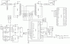
Regarding reclocking of the CS8412, I've set up options for FSYNC clocking at 44.1KHz, 48KHz, and 92KHz. I got the impression that SCK should be clocked at 64Fs, so that is what i've drawn in the scematic.. Sampling frequencies will be jumper programmable I guess...
CS8412 provides three outputs, the DATA, FSYNC, and SCK... PCM1792 recieves I2S on LRCK (pin 4), BCK (pin 6), and DATA (pin 5)....
wich goes where? and should clock the PCM1792 SCK?
I would like to be able to switch between 16 and 24 bit operation of the PCM1792, just as I'll be able to select sampling frequencies.. that means as far as I've understood switching the FMT[2:0] bits in control register 18 of the PCM1792, between 100 (16bit I2S) and 101 (24bit I2S)... Ehm.. do I need an MCU here? or can I get away with glue logic?
it will be clocked by the 11.2896MHz clock as far as I've understood.. But as you can read in this post I am not quite sure..
Should the flipflop be clocked to 256Fs if switching to 48KHz or 92KHz sampling frequency?
Regarding reclocking of the CS8412, I've set up options for FSYNC clocking at 44.1KHz, 48KHz, and 92KHz. I got the impression that SCK should be clocked at 64Fs, so that is what i've drawn in the scematic.. Sampling frequencies will be jumper programmable I guess...
CS8412 provides three outputs, the DATA, FSYNC, and SCK... PCM1792 recieves I2S on LRCK (pin 4), BCK (pin 6), and DATA (pin 5)....
wich goes where? and should clock the PCM1792 SCK?
quote from PCM1792 datasheet
Audio Serial Interface
The audio interface port is a 3-wire serial port. It includes LRCK (pin 4), BCK (pin 6), and DATA (pin 5). BCK is the
serial audio bit clock, and it is used to clock the serial data present on DATA into the serial shift register of the audio
interface. Serial data is clocked into the PCM1792 on the rising edge of BCK. LRCK is the serial audio left/right word
clock.
The PCM1792 requires the synchronization of LRCK and system clock, but does not need a specific phase relation
between LRCK and system clock.
If the relationship between LRCK and system clock changes more than ±6 BCK, internal operation is initialized within
1/fS and analog outputs are forced to the bipolar zero level until resynchronization between LRCK and system clock
is completed.
quote from PCM1792 datasheet
PCM Audio Data Formats and Timing
The PCM1792 supports industry-standard audio data formats, including standard right-justified, I2S, and
left-justified. The data formats are shown in Figure 28. Data formats are selected using the format bits, FMT[2:0],
in control register 18. The default data format is 24-bit I2S. All formats require binary 2s complement, MSB-first audio
data. Figure 27 shows a detailed timing diagram for the serial audio interface.
I would like to be able to switch between 16 and 24 bit operation of the PCM1792, just as I'll be able to select sampling frequencies.. that means as far as I've understood switching the FMT[2:0] bits in control register 18 of the PCM1792, between 100 (16bit I2S) and 101 (24bit I2S)... Ehm.. do I need an MCU here? or can I get away with glue logic?
rfbrw said:As I understand it, this is the input to a DAC. That being so, what signal do you intend to clock the FF with?
it will be clocked by the 11.2896MHz clock as far as I've understood.. But as you can read in this post I am not quite sure..
Attachments
Sure that you wanted comments.........?
What good does it do to reclock the incoming data, when it will go out with almost 1 n Sec of jitter, from the PLL????????
Why stick all those XOR gates in there to get differential, then put a transformer after it?
At least you have something between the '8412 and the line. Just the wrong stuff, in the wrong order.
Jocko
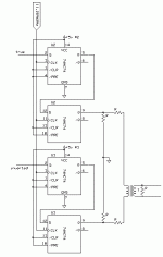
I realize the '86 was messed up in the 1st schem... I've got to xor signal with +5V to invert, and xor signal with ground for non-inverting...? I'm thinking 1100 xor 1111 = 0011, 1100 xor 0000 = 1100....... right? but Jocko.. can you give me a clear hint on how to do this? will I reclock first, then split, then step down voltage (resistor network), then transformer?
I realize I ask alot of really stupid questions, but this digital stuff is all new to me... I'm really trying to learn.. 🙁
I realize I ask alot of really stupid questions, but this digital stuff is all new to me... I'm really trying to learn.. 🙁
NO!
Put the reclocker on the TX side, where you already have (or should have), a good, clean clock.
On the RX side, you add a secondary PLL. Some guy who sometimes posts here sells one. (I know from personal experience that it works. Drawback: cost.)
Those chips may not like driving a resistive load................
The simple RX circuits that you can find on the web work ok. The TX ones do not.
Jocko
- Status
- Not open for further replies.
- Home
- Source & Line
- Digital Source
- Balanced SPDIF reciever?