Babys first Opamp Buffer / Preamp
Howdy,
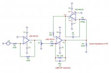
since i switched from Ananlog to a Digital Source i wanted to design my own preamp / buffer. The approach is very minimalistic, DC coupled, just one input and one output and a volume pot.
I am running a PCM5102 based DAC on an Odroid C1+, Vout is 2V RMS, my power Amps are Pass F5 Monoblocks, I need very little gain to drive the F5 to full swing. Looking at my parts bin i found some LME 49725 left overs and MAX44250 chopper amps.My first sketch had a RC Filter at the output, but output impedance was very high, so i implemented a simple servo using the chopper amp. The MAX44250 is very low noise (at least for a chopper) and this way i could get rid of all DC coupling caps, only 2 caps are left: C2 for HF supression and the 1u Filter cap in the servo.
I have attached the schematics below and will breadboard one channel before designing the PCB. Tight Resistor machting will be needed to ensure channel balance, but i can use a simple wheatstone bridge for that. I am not quite sure what kind of power supply i will use, but thats a problem for later.
My Question is: Does anyone see any major flaws in the design? Is C2 already to big since there will be also some cable capacity on the output. I will definately need some help with the PCB design, i will use star grounding for sure.
Howdy,
since i switched from Ananlog to a Digital Source i wanted to design my own preamp / buffer. The approach is very minimalistic, DC coupled, just one input and one output and a volume pot.
I am running a PCM5102 based DAC on an Odroid C1+, Vout is 2V RMS, my power Amps are Pass F5 Monoblocks, I need very little gain to drive the F5 to full swing. Looking at my parts bin i found some LME 49725 left overs and MAX44250 chopper amps.My first sketch had a RC Filter at the output, but output impedance was very high, so i implemented a simple servo using the chopper amp. The MAX44250 is very low noise (at least for a chopper) and this way i could get rid of all DC coupling caps, only 2 caps are left: C2 for HF supression and the 1u Filter cap in the servo.
I have attached the schematics below and will breadboard one channel before designing the PCB. Tight Resistor machting will be needed to ensure channel balance, but i can use a simple wheatstone bridge for that. I am not quite sure what kind of power supply i will use, but thats a problem for later.
My Question is: Does anyone see any major flaws in the design? Is C2 already to big since there will be also some cable capacity on the output. I will definately need some help with the PCB design, i will use star grounding for sure.
Attachments
Last edited:
While it's not terribly relevant in actual use at the end of the day, that input buffer / inverter would be quite noisy. Do you really need a 100 kOhm input impedance? Do the math - 1.4 pA/sqrt(Hz) * (100||100) kOhm = 70 nV/sqrt(Hz), leaving even the resistors' 28.5 nV/sqrt(Hz) in the dust. A humble TL072 or similar FET input part (e.g. AD712) would be more than 6 dB better, cutting output noise levels from 21.4 to 9.5 µVrms (or -99 dBFS to -106 dBFS re: 2V, respectively). If you're not sure about driving abilities, stack two.
Be sure to account for opamp input capacitance by a small cap across R2, typically 6 pF for a TL072. Can also be bigger, just watch out for bandwidth.
You are worrying about tight resistor matching when using a volume pot? Like, srsly? Do you know how much channel imbalance these tend to have?
What sort of volume pot value were you thinking of anyway, probably a 10k? For some reason, 50-100 kOhm jobs seem to give better channel balance than lower-impedance ones, though you'll want to run them a little hotter, with maybe a bit of gain in the input stage and correspondingly less (with higher-value resistors) afterwards. Don't overdo it, the input stage should have enough headroom for 0 dBFS level +2 dB or so. On +/-15 V, you could consider going +8 dB / -5 dB, and maybe +3 dB / 0 dB on +/- 9 V.
I don't see a problem with that 56p. If in doubt, nobody said you couldn't include 47-100 ohms of output series resistance anyway. Plenty low enough still, and gives you some short-circuit protection to boot.
I suggest you include something like 2k2-3k3 to ground after R7, in order to keep that resistor or the servo from dominating your output noise.
It's a bit unfortunate that this Maxim part is only good to +/-10 V max. You may have to provide two sets of supplies if +/-9 V doesn't cut it.
With a part like the LME49725 at hand, you might just as well consider playing it straight and going with plain ol' boring noninverting circuitry and sub-10k feedback loop impedances (with supply decoupling to match). The part has a bit too much current noise for use in higher-impedance (including typical inverting) circuits, but its common-mode and input impedance nonlinearity should be quite good. Plan B would be staying inverting but plastering the circuit with additional unity-gain buffer stages, so that feedback impedances can be reduced and overall noise is brought down.
Howdy,
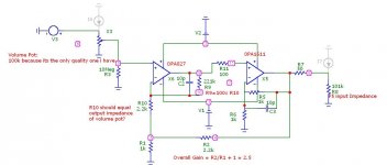
100k input Pot because this is basiclly a parts bin build, and i have only one high quality 100k pot. I read a lot of Walt Jungs Papers on line drivers and came up with the following aattached design. Its based on the composite current boost line driver two.
http://www.waltjung.org/PDFs/ADI_2002_Seminar_Ch6_Audio_Drivers_I.pdf
The circuit below simulates well, but i am not sure what value is needed for R10 and R9 since they should be based on the output impedance of the volume pot. The Gain of X2 should be: (Overall Gain / 2) -1. In my case that would mean 0.25, but with this configuration i cant go lower then 1, could this turn out problematic? I dont need a gain higher than 2.5, 3 at max.
Without R9/10 C2 its oscillation hell in simulation. Some feedback from the experienced builders would really be appreciated.
Attachments

Somewhere in Jung's papers he tells you the gain to use for the second opamp in the composite.
Achieving that gain allows you to set your R6 value.
Can the 49725 drive the 1k feedback resistor and the load?
Question: does the 1k5 (R2) form part of the load?
i.e. if the output load is 10k does the 49725 see 1k||1k5||101k||10k as the total loading?
Achieving that gain allows you to set your R6 value.
Can the 49725 drive the 1k feedback resistor and the load?
Question: does the 1k5 (R2) form part of the load?
i.e. if the output load is 10k does the 49725 see 1k||1k5||101k||10k as the total loading?
Somewhere in Jung's papers he tells you the gain to use for the second opamp in the composite.
Yes Jung states that gain of X2 should be: (Overall Gain / 2) -1
This requires a overall gain of 4 or higher for a unity gain X2 so: 4/2 -1 = 1. Thats a little to much gain for my needs, so my question is if there are problems using my chosen configuratiion.
The LME49725 should be able to drive the 1k, but the resistor value can be increased its just there to limit HF response, The LME49725 is a VF opamp, Jung uses CF opamps in the X2 position in one example circuit also as a unity gain follower without R6.
I have to admit in simulation i used a NE5534 model insted of the LME49725 since i have no model for that.
I didn't realise your "X2" was referring to that second stage.
Could the overall gain be the 64times of the first stage and the 2times of the second stage? Equals 120times, or does it refer to the closed loop gain of the composite?
Reading his advice (from about 3 years ago) seems to suggest it's the closed loop gain of the composite.
Could the overall gain be the 64times of the first stage and the 2times of the second stage? Equals 120times, or does it refer to the closed loop gain of the composite?
Reading his advice (from about 3 years ago) seems to suggest it's the closed loop gain of the composite.
Last edited:
I tried contacting Walt Jung directly but the contact page on his Blog is not working.
So the questions remain. Are there any major flaws in the design? Should R9 and R10 be increased since the original compensation is for a 50k pot, and last but not least, keep R6 or leave it out? I can put it in the PCB design just to make sure and just dont populate it.
Simulation is all fine, distorsion is definately lower with R6=1K so the second stage has a gain of 2.
I hate hate hate hate PCB design, and star grounding and ground busses and everything ground related. Where is ground bussing ok, where do i create substars and i dont know, even going for short path connections my layout looks like a cluttered mess.
So,
i read a lot about grounding and decoupling Opamp circuits. I guess it was about time i finally sit down and learn this stuff. I made some changes to the circuit. Opamps are now OPA827 for the input stage and OPA1611 for the output stage, i also added a small cap to limit the frequency response since the OPA1611 is pretty fast.
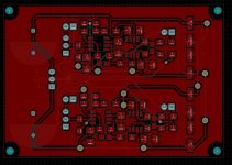
For grounding i went with a Ground plane for power GND and a star ground for signal GND. The PCB Design is done. Could somebody have a look at it? I cant attach KICAD files here directly, should i zip it or post jpgs?
i read a lot about grounding and decoupling Opamp circuits. I guess it was about time i finally sit down and learn this stuff. I made some changes to the circuit. Opamps are now OPA827 for the input stage and OPA1611 for the output stage, i also added a small cap to limit the frequency response since the OPA1611 is pretty fast.
For grounding i went with a Ground plane for power GND and a star ground for signal GND. The PCB Design is done. Could somebody have a look at it? I cant attach KICAD files here directly, should i zip it or post jpgs?
Attachments
I wonder if the Jung formula to determine the 2nd stage gain, is telling us that the second stage should be a unity gain buffer, when overall gain is less than, or equal to 4?
Following his papers i think it should be, on the other hand in some of his examples the second stage has a slightly higher gain in others not.
Since the design is based on his latest work on the topic i have the feeling that the second stage should be unity gain when the overall gain is lower then four but i really cant see any differences in simulation. I will check that later today at the moment i am doing some PCB optimization, shortening leads etc.
Since the design is based on his latest work on the topic i have the feeling that the second stage should be unity gain when the overall gain is lower then four but i really cant see any differences in simulation. I will check that later today at the moment i am doing some PCB optimization, shortening leads etc.
It seems a waste to operate a very high gain opamp at unity gain and the compromises that brings, when a unity gain buffer that is designed to operate best at unity gain gives at least equal performance.
The lme49600 datasheet shows tremendous performance.
The lme49600 datasheet shows tremendous performance.
according to the datasheet the lme49660 has a max Vos of 60mV, my F5 is DC coupled and i dont want my speakers to explode.
where did lme49660 enter the circuit?
and it's a composite.
The overall gain controls the output offset. i.e. the first stage reads the output and uses NFB to reduce errors.
and it's a composite.
The overall gain controls the output offset. i.e. the first stage reads the output and uses NFB to reduce errors.
Last edited:
It seems a waste to operate a very high gain opamp at unity gain and the compromises that brings, when a unity gain buffer that is designed to operate best at unity gain gives at least equal performance.
The lme49600 datasheet shows tremendous performance.
You suggested the use of a dedicated unity gain buffer here 😉
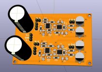
Here is the PCB Layout: Front, Back and 3D view. The binding posts are just placeholder, The caps on the right are aluminium polymer, decoupling caps C3 to C10 will be film types (No ceramics since i dont expect any HF to be supressed), all resistors 1206 since i really have problems soldering 0805 and i hate 0603.
Now diner, then some more simulations.
Now diner, then some more simulations.
Attachments
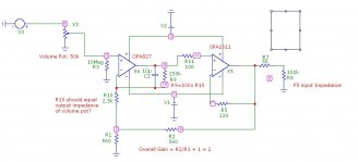
After an afternoon of simulation i have settled on the final values for the prototype. The second stage is now unity gain. R5 is lowered to 220 Ohm, this prevents HF spiking. For values larger then roundabout R5 > 1.5K oscillation occurs. The second capacitor has been removed in the schematics but i left the footprint on the PCB, maybe it might be needed, you never know. Distorsion in simulation has reduced by neaarly 50%. R1 and R2 were lowered to 560, overall gain is now 2, thats enough for my needs, this has also reduced noise.
R9 and R10 will be subject to experimentation, slightly higher values might be needed (4.7k / 470k).
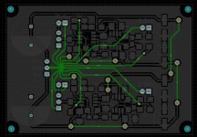
By removing R6 i was able to shrink the the PCB a little, especially the signal ground traces are now as short as possible and everything is a little more tidy.
Since everything looks good in simulation its now time to build a prototype and see how things work in real life or if the magic smoke escapes and everything sounds horrible. I guess this is part of the learning process, simulate, build, fail retry. I will send out the PCB files tomorrow and tournaround will be around 10 days, parts will be ordered tomorrow too. I will use the time to update my Sulzer reg to a Sulzer Boberly type. Expect the first results in two weeks or so
R9 and R10 will be subject to experimentation, slightly higher values might be needed (4.7k / 470k).
By removing R6 i was able to shrink the the PCB a little, especially the signal ground traces are now as short as possible and everything is a little more tidy.
Since everything looks good in simulation its now time to build a prototype and see how things work in real life or if the magic smoke escapes and everything sounds horrible. I guess this is part of the learning process, simulate, build, fail retry. I will send out the PCB files tomorrow and tournaround will be around 10 days, parts will be ordered tomorrow too. I will use the time to update my Sulzer reg to a Sulzer Boberly type. Expect the first results in two weeks or so
Attachments
- Status
- Not open for further replies.
- Home
- Source & Line
- Analog Line Level
- Baby first Opamp Buffer / Preamp