😄
I know, my use of "reverse" was not much appropriate. I only meant i inverted the probes.
I've also read about the use of the jfet as a diode, though I'm really still struggling understanding some things.
When the jfet is reverted, then, is it ok to get a much higher current? Did I damage them going over 20mA? And what about the different forward current values with 1,2 volts?
Sorry for the many questions. Asking because I measure a different resistance too, across them
Try this. The 1ohm lets you see the current easily. In the second image the inverted FET current is in the amps range because the gate to source/drain behaves as a diode. In the real three legged JFET the drain and source are indistinguishable and can be freely interchanged. They are notional markings only as the device is truly symmetrical. That only applies to 'most' JFET's and not any to any other kind of FET.


I wouldn't like to say if it has been damaged or impaired... although I think it will still function correctly in something like this. Not ideal though 🙂
This is a bit like how the JFET measures. So if you join the gate and one other leg then it will conduct heavily if you forward bias the diode.

I wouldn't like to say if it has been damaged or impaired... although I think it will still function correctly in something like this. Not ideal though 🙂
This is a bit like how the JFET measures. So if you join the gate and one other leg then it will conduct heavily if you forward bias the diode.
Attachments

Thank you very very much, Mooly.
I would not expect such a detailed explanation and I am now studying this matter.
I will change the jfet's.
I'm now thinking I checked the mosfets with a DMM that is not enough to reach the threshold V, then I'm looking to setup this .
In the meantime, I contacted Mouser and they can't guarantee me for 4 matched IRFP240 fet's. That's crazy.
Thank you!
I would not expect such a detailed explanation and I am now studying this matter.
I will change the jfet's.
The FET's are probably where the big variations are tbh.
I'm now thinking I checked the mosfets with a DMM that is not enough to reach the threshold V, then I'm looking to setup this .
In the meantime, I contacted Mouser and they can't guarantee me for 4 matched IRFP240 fet's. That's crazy.
Thank you!
Hmmm 🙂
A DVM probably wouldn't reach the gate/source threshold voltage which is around 4 volts give or take.
The procedure in that article is a bit open to interpretation.
Do you remove the screwdriver before taking the measurement? If you do then which pin do you lift the short from first. If you even touch just the gate with the screwdriver you will most likely apply charge which will stay there and might turn the FET on when you test it.
Fwiw most failures of power FET's are obvious, they fail short or almost short from Drain to Source.
The MOSFET Tester Jig is a bit brutal in implementation. The 1k on the gate is way to low imo.
A 1meg or 10 meg should be enough to fully turn the FET off. All it has to do is remove stray charge.
As for turning the FET on, if the 1k is removed and a 1 meg connected between gate and +9 volts the FET should turn full on. A direct switch connection could make a damaged FET appear OK when in fact it is anything but and has a gate/source leakage.
A DVM probably wouldn't reach the gate/source threshold voltage which is around 4 volts give or take.
The procedure in that article is a bit open to interpretation.
3) With a screwdriver or meter probe, short the gate and drain pins of the mosfet. This will initially keep the internal capacitance of the device completely discharged.
4) Now Touch the meter black probe to source and the red probe to drain of the device.
Do you remove the screwdriver before taking the measurement? If you do then which pin do you lift the short from first. If you even touch just the gate with the screwdriver you will most likely apply charge which will stay there and might turn the FET on when you test it.
Fwiw most failures of power FET's are obvious, they fail short or almost short from Drain to Source.
The MOSFET Tester Jig is a bit brutal in implementation. The 1k on the gate is way to low imo.
A 1meg or 10 meg should be enough to fully turn the FET off. All it has to do is remove stray charge.
As for turning the FET on, if the 1k is removed and a 1 meg connected between gate and +9 volts the FET should turn full on. A direct switch connection could make a damaged FET appear OK when in fact it is anything but and has a gate/source leakage.
Example. Look at the value of the gate resistor. It is a hundred million million ohms. Now you won't have one of those but it illustrates the point. The FET still turns full on as shown by Vout being approximately zero. The gate draws essentially no current at DC as FET's are voltage rather than current driven. So a 1meg or 10 meg is a good practical value as a test.

Attachments
I removed the screwdriver but honesty I didn't take care of which pin i lifted the short from first! I will desolder them again, to recheck.Do you remove the screwdriver before taking the measurement? If you do then which pin do you lift the short from first. If you even touch just the gate with the screwdriver you will most likely apply charge which will stay there and might turn the FET on when you test it.
Fwiw most failures of power FET's are obvious, they fail short or almost short from Drain to Source.
I didn't get a short from my tests. But it occurred to me now, after resoldering them in and while doing some measures with the test bulb (bulb is 60W), I checked the drop voltage between the various pins of mosfets to compare between the 4 of them and only on one fet (just on the channel where I could not adjust the bias) I saw the bulb lit up and the amp went into protection during the connection of probes. By the way: it sent the meter into protection too!
I need to study this more 🙂 . But thank you again!As for turning the FET on, if the 1k is removed and a 1 meg connected between gate and +9 volts the FET should turn full on. A direct switch connection could make a damaged FET appear OK when in fact it is anything but and has a gate/source leakage.
I checked the drop voltage between the various pins of mosfets to compare between the 4 of them and only on one fet (just on the channel where I could not adjust the bias) I saw the bulb lit up and the amp went into protection during the connection of probes.
If touching the gate of the FET while it is in circuit caused the lamp to light then I would guess either the amp went unstable due to the meter and meter lead parasitic capacitance or the FET gate is actually floating. Worth checking the continuity with the amp off.
The bulb should protect the FET's
That's what I did. I took the fet's apart and found no continuity. Neither when they are mounted
I should have checked better before. But sometimes frustration for being stuck brings to something.
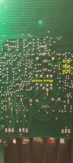
I've found out why the missing contact between top and bottom of the PCB, in one hole where the smoothing caps are soldered, causes the right channel to not changing from bias 0. In the pictures, the +44 voltage path to R115, R120, R121.
Mooly, thank you very much for all your help. Should you snip those resistors in LTSpice, you can have a confirm, because there won't be current in TCR504.
Still waiting for the copper PCB eyelets to arrive from China. I couldn't find the right size in Italy, neither online on big suppliers' web sites. Weird!
Attachments
Last edited:

Hi Mooly.
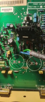
Brass eyelets have been fixed to restore the broken PCB side to side contact. I replaced the current regulator on both channels and some resistor that were out of specs. Now (always with the test bulb) R15 and R24 do burn on the left channel.
I started testing without remounting the bottom chassis. Is that a big mistake as the ground might not be connected for certain components? 😳
Moreover, I'm doubting about the jfet's D-g-kee sent me. Can it be there's not J504 written on?
Last edited:
I'm also wondering whether I damaged the polystyrene caps with the isopropyl alcohol or redoing all joints
Its only a mistake if 'might not be connected' becomes a definite 'not connected' 😉I started testing without remounting the bottom chassis. Is that a big mistake as the ground might not be connected for certain components?
R15 and R24 do burn on the left channel.
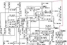
Standout symptom is R24. If that is burning then it suggests an issue around Q10.
If that constant current FET is faulty or suspect (in other words it is conducting heavily) then there is a direct path from the negative rail through R26 and then the B/E junction of Q10 into the 100 ohm to ground. In other words the 100 ohm is effective across the negative rail (if that FET is faulty).
The other possibility is a route from the positive rail but that would mean Q10 is faulty. The collector/base junction should withstand the full supply voltage and not conduct.
Measuring the voltage across the 100 ohm will confirm what is happening. If it is negative the current is coming from te negative rail.
So perhaps there is an issue with those parts. They need to be rated to withstand the full negative rail voltage which many common JFET's like the 2N3819 will not.
I'm also wondering whether I damaged the polystyrene caps with the isopropyl alcohol or redoing all joints
Unlikely. The iso shouldn't be an issue and you would have to really overheat the parts to melt and damage them. Normal reflowing the joints should not be an issue.
Mooly said:Its only a mistake if 'might not be connected' becomes a definite 'not connected' 😉
Sorry, my English is not as good as for understanding this. The holes the screws that connect the pcb to the bottom chassis go in are not surrounded by conductive layer. Anyay, I'll try agan while remounted
Mooly said:Standout symptom is R24. If that is burning then it suggests an issue around Q10.
If that constant current FET is faulty or suspect (in other words it is conducting heavily) then there is a direct path from the negative rail through R26 and then the B/E junction of Q10 into the 100 ohm to ground. In other words the 100 ohm is effective across the negative rail (if that FET is faulty).
The other possibility is a route from the positive rail but that would mean Q10 is faulty. The collector/base junction should withstand the full supply voltage and not conduct.
Measuring the voltage across the 100 ohm will confirm what is happening. If it is negative the current is coming from te negative rail.
So perhaps there is an issue with those parts. They need to be rated to withstand the full negative rail voltage which many common JFET's like the 2N3819 will not.
I'm doing these tests now, after replying here. Though, to my limited knowledge, LTSpice gives a really small but anyway negative voltage across R24
What I ordered from DGkey is just this, then it should be ok, unless they sent me the wrong one but I doubt this. What I disappointedely notice is the resistance across the 2 new jfet's was not the same 😏
My big mistake: on this channel, I soldered the J504 with opposite pins! Now, though, the two resistors keep on blowing.
With the 60W bulb in series, this is what I measure at the leads of R24 and R15 (DMM on DC V range):
R24: -6 and -22V
R15: 36 e -31V
With the 60W bulb in series, this is what I measure at the leads of R24 and R15 (DMM on DC V range):
R24: -6 and -22V
R15: 36 e -31V
Last edited:
- Home
- Amplifiers
- Solid State
- Arcam Delta 290 Mains And Power Stage On LTSpice