Lenon89 has a better schematic.
Update on mine from yesterday, as it's the same issue. I've tried to figure out where this voltage comes from on pin 16 (tl494).
I'm referencing to my schematics.
I've lifted D1, D2, D5, D6 and also R31 and R28 - voltage still there at pin16. 😕
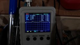
I took my scope i and look at pin16. It's not a pure DC it's something like a pulses of a sawtooth wave 😱😕
I'm also a little bit confused. Perry by your manual:
Pin 5 is the timing capacitor (Ct) terminal. Pin 6 this pin is for the timing resistor (Rt).
But in the schematics i've posted it's the other way around. 😕

Lift all transistors or any other components that can drive voltage to pin 16. You can remove them one at a time or all, then reinstall them one at a time to find which direction to go in troubleshooting.
I still can't wrap my head around why the amp does the same with a brand new driver board....
I will do what Perry says. Will remove Q8 and Q9 by my schematics and see what happens.
But i can confirm PIN 5 has RESISTOR and PIN 6 HAS CAPACITOR, shouldn't they be the other way around ?
I will do what Perry says. Will remove Q8 and Q9 by my schematics and see what happens.
But i can confirm PIN 5 has RESISTOR and PIN 6 HAS CAPACITOR, shouldn't they be the other way around ?
Do you have a normal sawtooth waveform on pin 5 with an amplitude of about 3.4v?
What is the DC voltage on pin 6?
What is the DC voltage on pin 6?
Pin 6 does go to a resistor. R99. 3.6 v.
Pin 5 does go to a capacitor. C46. Clean sawtooth waveform. 3.4v.
Pin 16 has 14v on it. Checking To find the source.
Pin 5 does go to a capacitor. C46. Clean sawtooth waveform. 3.4v.
Pin 16 has 14v on it. Checking To find the source.
Do you have a normal sawtooth waveform on pin 5 with an amplitude of about 3.4v?
What is the DC voltage on pin 6?
Pin 5 - stable 1.62vrms normal sawtooth waveform
Pin 6 - don't remember will double check later
After the ps driver board swap with a new one, now I have this at pin 16 😕
Attachments
Problem solved. Q50 was open. Replaced and out of protect. Thank Perry and Linen89 for all the help.
- Home
- General Interest
- Car Audio
- APSM-1500 In Protect