Iwas wondering if anyone has tried this?
I found it on ebay. you email them gerber and nc in UK then they send it off to china and it comes back in a week or so.
http://cgi.ebay.ca/PCB-Printed-Circ...4QQihZ019QQcategoryZ36323QQrdZ1QQcmdZViewItem
it is MUCH cheaper than expresspcb etc. probably as cheap as making boards yourself.
I found it on ebay. you email them gerber and nc in UK then they send it off to china and it comes back in a week or so.
http://cgi.ebay.ca/PCB-Printed-Circ...4QQihZ019QQcategoryZ36323QQrdZ1QQcmdZViewItem
it is MUCH cheaper than expresspcb etc. probably as cheap as making boards yourself.
I currently have some winging their way to me from China.
Its the 1st time I've had some manufactured (I'm quite new around here) so I'm not sure I'll be able to give much insight as to how they compare to others.
I'll see if I can get a photo up here when they turn up.
Mike
Its the 1st time I've had some manufactured (I'm quite new around here) so I'm not sure I'll be able to give much insight as to how they compare to others.
I'll see if I can get a photo up here when they turn up.
Mike
Christer said:Have you checked out Olimex? They are cheaper as far as I can see.
http://www.olimex.com/pcb/
I think this could be a good option.
And this Bulgarian company has existed for 15 years now.
And has a rather many costumers.
So I think it is trustworthy and reliable.
http://www.olimex.com/about.html
General Information
Olimex Ltd is private company,
with capability to design, prototype and manufacture
- printed circuit boards,
- sub-assemblies and
- complete electonic products.
The company is established in 1991 in Plovdiv - the second biggest city in Bulgaria.
.................
Olimex is recognized as 3rd party hardware developer from
- Texas Instruments Inc.,
- Maxim-Dallas Inc.,
- Atmel Inc.,
- Philips Semiconductors Inc.,
- ST Microelectronics Inc.,
- IAR Systems AB,
- Cirrus Logic Inc. ,
- OKI Semiconductor Inc.
...and have over 3000 active customer accounts
which regularly use our services for electronic boards development and prototyping.
lineup
Only reason I never used olimex is their requirement that you fax your credit info to them. I don't have a landline (for 5 years now) and I can't think of any other company that does this.
dietcoke said:... olimex is their requirement that you fax your credit info to them ...
sounds a bit strange and difficult
not all have a fax or can send fax
they not accept email?
christmas
lineup
lineup said:
sounds a bit strange and difficult
not all have a fax or can send fax
they not accept email?
christmas
lineup
There are internet fax services available.
I could not see any reference to PTH. Was this carefully avoided or asumed ??
What is PTH, plated through-hole? Their prototype boards have it. I used Olimex for my JLH amp and were quite satisfied. However, there are no small components on this board. I know others here have used them, try a search for more info.cliff said:
I could not see any reference to PTH. Was this carefully avoided or asumed ??
Also, Olimex built the STR9 microcontroller eval board we are using at work, and it looks fine.
cliff said:
I could not see any reference to PTH. Was this carefully avoided or asumed ??
PaulB - yes I just learned by search with google 😀 that
PTH = Plated-Through-Hole
Not only do they support PTH at www.Olimex.com
they also give good and very detailed design tips!
based on 15 years doing thing like this for custumers.
------------ quote ----------------------------------------------------------
#1 Silkscreen Outlines
Don't place silkscreen outlines on the solder pad area
Use silkscreen line widths which meet your PCB manufacturer's requirements.
#2 Holes
If the board is double sided the plating will decrease the holes with 0,1 mm
The component lead - hole clearance have to be 0,2 - 0,4 mm
If your board will be assembled by automat use clearance in the upper limit.
Clearance > 0,5 mm may cause unfilled pads (especially for single side PCB)
Clearance < 0,3 mm for PTH boards make difficults flux gases to escape and
may cause unfilled pads by machine soldering. (well this pretty well depend on the flux used)
Try to standartize the hole sizes you are using,
don't use many drill sizes with 0,1 mm difference, or be ready to pay for this 😉
Schematic Routing
Use TOP view when design boards with only PTH components and
BOTTOM view when design with only SMT components
#3 Pads
If you are designing single side board use bigger pads as they have to keep the component's load.
We recommend you anual rings about 40-50 mils if the board is single side and exposed to vibrations.
Use oblonged or rectangular pads to enlarge the pad area for IC and components with the board is densite.
Use thermal bridges when the pads are in copper area.
The minimum annual ring (pad-hole) have to be = hole + 2 * min track width of your PCB manufacturer.
---------------- quote --------------------------------
websource: http://www.olimex.com/pcb/dfm.html
christmas
lineup
cliff said:Sorry, I was talking about PTH on the Chinese "hello proto" web-site.
cliff
I am sorry, too

I should have known .... and understood
Let's Both Get Happy! .. again
After all, it is C H R I S T M A S
..... so
! Don'T WorrY .. BE HappY !

lineup
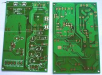
as promised, here is a pic (must get a decent digi-camera soon instead of my mobile-phone) of the boards I had made up.
Initial impressions are good. There are plated through holes.
Negative aspects are: no silkscreen on bottom (this was probably my fault due to inexperience),
the drilling for one of the mounting holes was slightly out & too close to edge (see arrow)
and finally the top silkscreen is a bit patchy in one or two places.
Now wheres that soldering iron......
Attachments
pinkmouse said:Was the mounting hole your error or theirs?
definitely theirs
I also noticed the boards are slightly different in size - only about 1 mm in it tho'
is the hole in the right place but the board is too small (size difference) or do the holes in the 2 boards not line up if u put them on top of each other?
neutron7 said:is the hole in the right place but the board is too small (size difference) or do the holes in the 2 boards not line up if u put them on top of each other?
having re-checked this, have come to the conclusion that the hole is actually in the right place, its just that the board hasn't quite been cut square.
Yes the holes do all line up between both boards.
In hindsight, maybe allowing only 1.5mm gap between edge of hole and board edge was a bit optimistic. ....
Anyway, reasonably pleased with result - obviously alot better than I could produce myself
p.s. thanks someone for un-moderating me - can now edit my posts 🙂
- Status
- Not open for further replies.
- Home
- Design & Build
- Parts
- Anyone tried "hello proto" PCB service?