Hi,
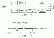
I am currently designing modulator board with two TAS5076 modulators. ABD delay parameter is indeed intended for distortion reduction but it's function is to actually delay one leg of half bridge in respect to the the other leg of the same full bridge. In this way simultaneous switching of both legs at around 50% duty cycle (low amplitude signal) is avoided with detrimental crosstalk effects. This is clearly depicted in attached picture from patent application US20020060605.
I have another problem. My aim is to make a multiphase power stage for the amplifier. So I will use one TAS5076 for left channel and one for the right. By feeding all channels with identical data and using interchannel delays and ABD delays I can have 12 phase power stage. What I do not know is this:
Is it possible to delay (phase shift) pwm outputs of any TAS5xxx modulator by delaying LRCLOCK and SDATA input? I use 192kHz LRCLOCK and PWM frequency is 384KHz. I assume that by delaying SDATA and LRCLOCK by 8 ticks of SCLOCK (12.288 MHz), then resulting phase shift would be 64 ticks of HFCLOCK (98.304 MHz) or 25% of PWM frequency (each PWM cycle consists of 256 ticks of HFCLOCK). I am asking this because I have allready board routed with 3 x TAS5015 modulators which would have mentioned phase shifted LR clocks, but I was not sure about the principle and also I had hard time finding suitable low jitter 98.304 or 100MHz can oscillator. I finally gave that up in favour of TAS5076 that has internal PLL and most important adjustable interchannel delay, but I would like also give TAS5015 a spin. I would like opinion, but if anyone with already working board is able to measure anything that would be great.
BTW, since modulator board will be separated from the power stage and I will need to route 12PWM channels for each amplifier channell I was toying with the idea of applying Brian's SERDES idea to PWM data. In this way PWM data is also reclocked. There are many chips that can do this, but the resulting gigabit rates scared me away. I have no tools to detect such datarates, even my spectrum analyzer goes only up to 1.5 GHz.
I would also like to mention, that I intend to use multiphase BCA power stage and not classical half bridges. Therefore I will only have 12 FETs to drive instead of 24 and no deadtime worry.
Best Regards,
Jaka Racman
The TAS5015 / TAS5012 use external capacitors to set the H-bridge deadtime. The TAS5076 has a digital adjustment (ABD Delay parameter). I like the idea of being able to easily tweak this value. This could be especially useful when matching the amp to a specific speaker driver. The ABD Delay parameter could be tweaked for minimum distortion using MLS measurements.
I am currently designing modulator board with two TAS5076 modulators. ABD delay parameter is indeed intended for distortion reduction but it's function is to actually delay one leg of half bridge in respect to the the other leg of the same full bridge. In this way simultaneous switching of both legs at around 50% duty cycle (low amplitude signal) is avoided with detrimental crosstalk effects. This is clearly depicted in attached picture from patent application US20020060605.
I have another problem. My aim is to make a multiphase power stage for the amplifier. So I will use one TAS5076 for left channel and one for the right. By feeding all channels with identical data and using interchannel delays and ABD delays I can have 12 phase power stage. What I do not know is this:
Is it possible to delay (phase shift) pwm outputs of any TAS5xxx modulator by delaying LRCLOCK and SDATA input? I use 192kHz LRCLOCK and PWM frequency is 384KHz. I assume that by delaying SDATA and LRCLOCK by 8 ticks of SCLOCK (12.288 MHz), then resulting phase shift would be 64 ticks of HFCLOCK (98.304 MHz) or 25% of PWM frequency (each PWM cycle consists of 256 ticks of HFCLOCK). I am asking this because I have allready board routed with 3 x TAS5015 modulators which would have mentioned phase shifted LR clocks, but I was not sure about the principle and also I had hard time finding suitable low jitter 98.304 or 100MHz can oscillator. I finally gave that up in favour of TAS5076 that has internal PLL and most important adjustable interchannel delay, but I would like also give TAS5015 a spin. I would like opinion, but if anyone with already working board is able to measure anything that would be great.
BTW, since modulator board will be separated from the power stage and I will need to route 12PWM channels for each amplifier channell I was toying with the idea of applying Brian's SERDES idea to PWM data. In this way PWM data is also reclocked. There are many chips that can do this, but the resulting gigabit rates scared me away. I have no tools to detect such datarates, even my spectrum analyzer goes only up to 1.5 GHz.
I would also like to mention, that I intend to use multiphase BCA power stage and not classical half bridges. Therefore I will only have 12 FETs to drive instead of 24 and no deadtime worry.
Best Regards,
Jaka Racman
Attachments
Hi Jaka,
Why don’t you just use 1 PWM output and use shift registers to Phase Shift the DATA?
With the TAS5015, you have 256 Bits per Cycle, so by using a 16 Bit shift register you delay by 1/16th of a cycle, having 16 of these in a series, you have 16 outputs each output +1/16th of a cycle. Something like a pair of 74VHC164 for each 16 bit Tap.
However, I personally believe this to be a bad idea, no matter how good your PCB layout is, the thought of have a large number of power stages operating, and trying to achieve low phase noise is just not going to happen. How would you de-couple them properly? Just the size of the PCB with the inherent tracking inductance would make this scheme a nightmare! Not to mention trying to track 16 PWM data lines while limiting Phase Noise and pulse width distortions.
I speak from personal experience with a similar scheme I used in a SAA7350 DAC designed 10 years ago, sounded good, but had poor dynamic range and THD due to the limitations on PCB layout – trying to track the Critical PDM data, while limiting Phase Noise and pulse distortion on these lines was imposable.
Best Regards,
John
Hi John,
Well, I have thought about it initally, but 30VHC chips would also be a layout nightmare. If there was something like high speed 4517 that would be another story. Also CPLDs are not efficient (one macrocell for each tap) and FIFOs are overkill.
I just thought it would be simpler to phase shift slower SCLOCK with less taps.
I have no argument against that except that I see my project more as an engineering exercise ( that no employer would pay for) than a high quality amplifier. Its final goal (very distant) is more in line with very high power amplifier (several kW) than a high quality one.
I would still like to know what do you think about feasibility of the original idea?
Best regards,
Jaka Racman
Something like a pair of 74VHC164 for each 16 bit Tap
Well, I have thought about it initally, but 30VHC chips would also be a layout nightmare. If there was something like high speed 4517 that would be another story. Also CPLDs are not efficient (one macrocell for each tap) and FIFOs are overkill.
I just thought it would be simpler to phase shift slower SCLOCK with less taps.
However, I personally believe this to be a bad idea, no matter how good your PCB layout is, the thought of have a large number of power stages operating, and trying to achieve low phase noise is just not going to happen. How would you de-couple them properly? Just the size of the PCB with the inherent tracking inductance would make this scheme a nightmare! Not to mention trying to track 16 PWM data lines while limiting Phase Noise and pulse width distortions.
I have no argument against that except that I see my project more as an engineering exercise ( that no employer would pay for) than a high quality amplifier. Its final goal (very distant) is more in line with very high power amplifier (several kW) than a high quality one.
I would still like to know what do you think about feasibility of the original idea?
Best regards,
Jaka Racman
Hi Jaka,
30 74VHC164’s is a lot, but in comparison to 16 output stages – it’s only two 164’s per Tap.
I would worry about the phasing of three TAS5015, how could you guarantee that all three would come out of reset and be “in phase” each power-up cycle? Maybe they would – I don’t know. The TAS5076 seems a better solution – at least the phase between “Taps” can be guaranteed.
Pls. clarify: - With a modulator with 256 “Bits” (by “Bits” I mean discrete time slots) would not the net sum of 16 output taps equally shifted by 16 “bits” be zero? After all a shift of 128 “Bits” is 180Deg😕
BR
John
Hi John,
Originally I was thinking about 6-8phases and that still needs 30 chips. I came to 12phases only because TAS5076 provides them.
Regarding multiphase approach here is an article that originated my design. Here is a patent application that further convinced me about validity of my project.
Thanks for your opinion, I think I will ditch multiple TAS5015 idea. VHC164 approach is still in consideration, but maybe it would be better to put it to the power stage.
BTW, one final question. Does TAS5015 already incorporate ABD delay like TAS5076?
Best regards,
Jaka Racman
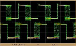
I'm not sure what you mean by ABD delay. However, the TAS5015 seems to have BD outputs - where the B channel PWM output is a 180Deg phase shift copy of the A channel (so delayed by 128 MCLK cycles). As opposed to AD modulation, where the B channel is a simple phase inversion of the A channel.
Below is a scope shoot of the TAS5015 A and B channels. The scope is triggered on Ach, the resultant "BD" modulation can be seen on the edges.
Below is a scope shoot of the TAS5015 A and B channels. The scope is triggered on Ach, the resultant "BD" modulation can be seen on the edges.
Attachments
Re: Yep... Still busy...
Well, heck, how hard is it to hook up a couple batteries, anyway 🙂
Actually, since I'm pretty certain that battery power will be suitable for my power requirements, the lack of power supply doesn' t bother me too much. I've got a few 12V SLA's on the way to experiment with on my XR10/25 units to make sure, though.
Well, I already have an XR25, and to be honest the reason the EVM is attractive to me is that I've had a look inside the XR25 🙂 It's nowhere near as mod-friendly as the XR-10. Given my complete lack of experience on SMD devices, as well as the fact that at least some I2C initialization is needed for the 5036, I'm not highly confident of my ability to hack the 25 into a suitable form without blowing it up. Since the EVM has handy-dandy headers and the ability to control much of the unit from a PC (which will be my only real source for my project), it seems to suit my abilities much better.
Well, this would be the other reason that the EVM is attractive - it seems to have rather better specs than the XR25/45, although it's not clear how much the Panasonic units are comprimised by their power supplies. Still, if you have to start somewhere, might as well start with the better base platform.
My primary goal is simply to get to the point of having a 6-channel direct I2S input. If the XR-10 had 6 channels rather than 5, I'd just use that. However, the ease of experimentation is attractive with the EVM, and you can do it without necessarily having to break out the soldering iron every time.
BTW - Related to JohnW's comments that the SRC in the TI chips isn't all that great, has anyone tried to compare the performance of the Panny units at different sampling frequencies? ie use a high-quality offline software SRC to upsample a CD to 96 and A/B it with the standard 44.1?
Brian Brown said:I've been looking at that new EVM as well.
The one thing that I've always been disappointed with TI's digital amp EVMs is that they don't include a reference power supply, one of the biggest quality variables.
Well, heck, how hard is it to hook up a couple batteries, anyway 🙂
Actually, since I'm pretty certain that battery power will be suitable for my power requirements, the lack of power supply doesn' t bother me too much. I've got a few 12V SLA's on the way to experiment with on my XR10/25 units to make sure, though.
The SA-XR25 / SA-XR45 use TAS5036 / TAS5182 chipsets. I don't have one of these receivers, but I've reviewed their schematics. The SA-XR25 is less than half the cost of TI's development board. The TAS5076 appears to be pin compatible with the TAS5036. Hacking into one of these receivers might be something to consider as an alternative.
Well, I already have an XR25, and to be honest the reason the EVM is attractive to me is that I've had a look inside the XR25 🙂 It's nowhere near as mod-friendly as the XR-10. Given my complete lack of experience on SMD devices, as well as the fact that at least some I2C initialization is needed for the 5036, I'm not highly confident of my ability to hack the 25 into a suitable form without blowing it up. Since the EVM has handy-dandy headers and the ability to control much of the unit from a PC (which will be my only real source for my project), it seems to suit my abilities much better.
The new six channel TAS5076 modulator chip looks very interesting. It appears to have better specs than all but the TAS5015 (which doesn't have an internal PLL). Previously the TAS5012 had the 2nd best specs.
Well, this would be the other reason that the EVM is attractive - it seems to have rather better specs than the XR25/45, although it's not clear how much the Panasonic units are comprimised by their power supplies. Still, if you have to start somewhere, might as well start with the better base platform.
My primary goal is simply to get to the point of having a 6-channel direct I2S input. If the XR-10 had 6 channels rather than 5, I'd just use that. However, the ease of experimentation is attractive with the EVM, and you can do it without necessarily having to break out the soldering iron every time.
BTW - Related to JohnW's comments that the SRC in the TI chips isn't all that great, has anyone tried to compare the performance of the Panny units at different sampling frequencies? ie use a high-quality offline software SRC to upsample a CD to 96 and A/B it with the standard 44.1?
Finished 5012 5110 amp
Just finished a cofiguration mentioned above. Sounds great and is very stable.
Sounds even beter when connecting the drivers direct to the 5110 instead of the neccesary EMI and carrier filters. Sound gets more direct and crisp.
Spdif gets unstable using very bad cable. One can't hear it, untill someone switches on the light or other elec. device. Than the amp goes into mute. Using better cable it's rocksteady.
Thing is, I used different types of psu's but the difference is hard to tell. So Brian, what do see as a good supply? I want to improve and built a better supply than my standard lab. psu. I was thinking of the classical LM117 with 4 parallel power transistors. Good decoupling and 4 parallel tantalum caps of 270 U, 13mOhm between the rails. Suggestions?
Next project will be 5015 and 5182 together. What is the problem with the 5015 except for the external PLL? Do I miss something? It seems quite the same as the 5012.
And, is it possible to use larger mosfets? 5182 checks driver voltage at pins 49,52,53. Increasing voltage with heavier fets would damage the 5182?
Re: Finished 5012 5110 amp
Congratulations! Is this a complete DIY design? If so, hats off to you, as it is far from trivial.
What kind of parts did you use in the reconstruction filter? I would imagine that this is the one place in an Equibit based design where parts quality can make a significant difference. Also, as Brian has pointed out way earlier in this thread, there are probably benefits to be gained by tuning the reconstruction filter values to the specific speaker being used.
Sounds like an obvious progression. I have to admit that JohnW's work has made me very interested in the 5015, but I don't really have the skill or time to consider a full layout myself.
Some of the clock-related discussions did get me thinking a bit about what the 'optimal' clock strategy would be when using one of the non-5015 parts where you're constrained to use the internal pll for clock recovery. I see 3 basic strategies:
1) 'conventional' where an SPDIF receiver or other I2S source is used to generate the clocks
2) SRC (TI4192 is the obvious choice) driven by a local clock, with the 50xx in slave mode using the clock output of the SRC
3) run the 50xx in master mode from a local low-jitter clock, and use the output clocks from the modulator to drive a SRC.
approach 2 is more or less what Brian is doing in his multichannel digital link, and given the poor performance of the oversampling filter in the modulators, I'd expect it to be noticibly better than approach 1 even aside from jitter considerations. However, it seems to me that approach 3 should have the potential to be even better, although much will depend on the implementation details.
Any thoughts? Since even the new 5076 evm appears to have the modulator hard-wired into slave mode, it doesn't seem like something that is seen as an expected/typical topology so maybe there is no merit to it. Seems like an interesting possibility, though.
Pitch254 said:Just finished a cofiguration mentioned above. Sounds great and is very stable.
Congratulations! Is this a complete DIY design? If so, hats off to you, as it is far from trivial.
Sounds even beter when connecting the drivers direct to the 5110 instead of the neccesary EMI and carrier filters. Sound gets more direct and crisp.
What kind of parts did you use in the reconstruction filter? I would imagine that this is the one place in an Equibit based design where parts quality can make a significant difference. Also, as Brian has pointed out way earlier in this thread, there are probably benefits to be gained by tuning the reconstruction filter values to the specific speaker being used.
Next project will be 5015 and 5182 together. What is the problem with the 5015 except for the external PLL? Do I miss something? It seems quite the same as the 5012.
Sounds like an obvious progression. I have to admit that JohnW's work has made me very interested in the 5015, but I don't really have the skill or time to consider a full layout myself.
Some of the clock-related discussions did get me thinking a bit about what the 'optimal' clock strategy would be when using one of the non-5015 parts where you're constrained to use the internal pll for clock recovery. I see 3 basic strategies:
1) 'conventional' where an SPDIF receiver or other I2S source is used to generate the clocks
2) SRC (TI4192 is the obvious choice) driven by a local clock, with the 50xx in slave mode using the clock output of the SRC
3) run the 50xx in master mode from a local low-jitter clock, and use the output clocks from the modulator to drive a SRC.
approach 2 is more or less what Brian is doing in his multichannel digital link, and given the poor performance of the oversampling filter in the modulators, I'd expect it to be noticibly better than approach 1 even aside from jitter considerations. However, it seems to me that approach 3 should have the potential to be even better, although much will depend on the implementation details.
Any thoughts? Since even the new 5076 evm appears to have the modulator hard-wired into slave mode, it doesn't seem like something that is seen as an expected/typical topology so maybe there is no merit to it. Seems like an interesting possibility, though.
Thanks for the hat off!
By "mentioned above" I ment the title of my reply, but it's not in the posting as well as the picture I attached (moderator?)so to make things clear:
Just finished 5012 / 5110 amp based on a evm design by TI. No XL25 or so involved. Created the pcb and the schematic by my self. Hopefully that's enough DIY.
Recon. filter is built with smd resistors and Wima caps. Just standard stuff. I can pick up the signal before this filter and design all kinds of expensive filtering, but I don't see why: the sound is great and I still say: less parts is more!
The drivers needs to dissipate an extra 1 watt carrier signal and my Mangers seems to have no problem with that. Don't know what is does for EMI, I think the worst. But sinds the amp will be placed inside the speakers, I think I can tackle that problem by extensive shielding.
About the the clock: you summarized it well, got to study the 4192. More on that later. Perfect PLL / osc. seems to be very important according JohnW.
Somebody suggestions on a PSU? I'm thinking of an LM117HV reg. with power trans. But the lm117hv is difficult to get.
Attachments

Lot's of replies to catch up with...
John, I've been following your posts on clocks and modulator IC evaluation with much interest. I'll have some more questions and comments on clocks coming. Here's a question on your modulator testing:
Are you testing the outputs of the modulator ICs directly (i.e. without a power stage)?
If so, are you using any type of reconstruction / low pass filter, such as an opamp stage?
I would be curious as to how such testing would compare to driving a 'real-world' load with a power output stage driving driving a reactive loudspeaker driver. I suspect that since these are open loop designs without feedback, that the results would be less susceptible to driver loading. On the other hand, some modulator chips have features to compensate for output stage variances (such as the ABD delay and DC offset parameters being discussed). I think that these might have significant value to an actual design.
Thanks for sharing your findings!
Brian.
JohnW said:I’ve been evaluating digital modulators from Zetex, TI & Sony. All have been externally Re-latched using an external low phase clock circuit.
Here’s a brief round up of the results, all Dynamic Range results are Awtd and are about –2dB worse then optimal due to poor phase noise of the LVDS RX / TX used on the common Eval board.
John, I've been following your posts on clocks and modulator IC evaluation with much interest. I'll have some more questions and comments on clocks coming. Here's a question on your modulator testing:
Are you testing the outputs of the modulator ICs directly (i.e. without a power stage)?
If so, are you using any type of reconstruction / low pass filter, such as an opamp stage?
I would be curious as to how such testing would compare to driving a 'real-world' load with a power output stage driving driving a reactive loudspeaker driver. I suspect that since these are open loop designs without feedback, that the results would be less susceptible to driver loading. On the other hand, some modulator chips have features to compensate for output stage variances (such as the ABD delay and DC offset parameters being discussed). I think that these might have significant value to an actual design.
Thanks for sharing your findings!
Brian.
Jaka Racman said:I am currently designing modulator board with two TAS5076 modulators. ABD delay parameter is indeed intended for distortion reduction but it's function is to actually delay one leg of half bridge in respect to the the other leg of the same full bridge. In this way simultaneous switching of both legs at around 50% duty cycle (low amplitude signal) is avoided with detrimental crosstalk effects. This is clearly depicted in attached picture from patent application US20020060605.
Yes,
I now realize that I was confusing the ABD delay (in the modulator) with the dead time adjustment set by resistors to BIAS-A and BIAS-B in TI's output chips (DTC_HS and DTC_LS on the TAS5182).
The TAS5015 and TAS5012 have the ABD delay fixed, with no adjustment possible.
Another thought that pops to mind is that it might be beneficial to use pots for the deadtime adjustment (at least initially) to tweak for minimum distortion.
Brian.
Jaka Racman said:I have another problem. My aim is to make a multiphase power stage for the amplifier. So I will use one TAS5076 for left channel and one for the right. By feeding all channels with identical data and using interchannel delays and ABD delays I can have 12 phase power stage.
This is getting into an area of Equibit modulation and noise shaping that I don't fully understand.
I had thought that part of the Equibit scheme made some type of compensation for the ClassAB-like zero crossing that occurs with H-Bridges switching at low signal levels.
It sounds like using the interchannel delay would make it possible to drive a multi-phase output. One concern I have is that since multiphase wouldn't need zero crossover compensation, it might actually result in higher distortion.
If your main concern is high power, then perhaps this wouldn't be a problem.
What I do not know is this:
Is it possible to delay (phase shift) pwm outputs of any TAS5xxx modulator by delaying LRCLOCK and SDATA input?
I don't know.
It isn't clear to me that there is a fixed group delay that you could count on to do this. It probably would require some experimentation.
BTW, since modulator board will be separated from the power stage and I will need to route 12PWM channels for each amplifier channell I was toying with the idea of applying Brian's SERDES idea to PWM data. In this way PWM data is also reclocked.
I've thought about sending the PWM from the modulator to the power stage over a SerDes link, but I haven't tried it yet.
Just as John's experiments show performance effects of the modulator's clock quality, the quality of the recovered SerDes clocks at the power stage will affect performance. (In this scenario, a master clock would have to be at the modulator instead of at the output stages).
This isn't to say that it's a bad idea. In fact, I think that it's possibly an approach that offers a very good balance of compromises.
I have many thoughts and questions regarding possible topologies of clock sources, clock distribution, location of modulators, power stages, etc.
More on this to follow...
Brian.
More on the TAS5076 / TAS5012
I had made an earlier comment about the TAS5076 having better specs than the TAS5012.
Specifically, the TAS5076 has better THD+N and dynamic range 'specs'. However...
Looking at the data sheets again, the TAS5012 only talks about these values on the front page. There are no 'real' specs.
The TAS5076 reports 'system' specs combined with a TAS5182 design. (I think much of TI's earlier reporting on the TAS5012 was also with an earlier output stage, such as the TAS5110.)
In other words, I don't think that a valid quality comparision can be made between these chip series based on TI's published info.
I'm not aware of any direct statements made by TI comparing the performance quality of the TAS5012 to the TAS5076. If anybody knows of some, please share it.
The only comparison conclusions I *can* make at this time are the following:
The TAS5012 is TI's current best two-channel modulator with an internal PLL.
The TAS5015 is TI's current best two-channel modulator overall (relying on a higher quality external clock).
The TAS5076 is TI's current best six-channel modulator (I also note that it offers a choice of using the internal PLL or an external clock).
One thing that slightly concerns me is that the TAS5076 has slightly poorer dynamic range specs for four of the six channels (as tested with their EVM board). The EVM board has equivalant output sections for all six channels. To me this implies that the TAS5076 doesn't have equivalent modulator sections for all channels. It's not a big difference, but I have a personal hang-up about wanting stuff to match.
Brian.
Re: Re: Yep... Still busy...
That's cool.
There are a couple of questions I have:
Can you tell if the Equibit board in the SA-XR25 is made by TI or Pansonic?
I don't have the SA-XR25 schematics handy to recheck. When I had initially examined them it looked like the SA-XR25 used a fixed voltage power supply (the SA-XR10 uses a variable supply). I recently saw on Panasonic's website a statement that the SA-XR25 uses a variable supply. Would it be possible for you to check this out?
I'm using an ASRC in my interface to my digital amp. Subjectively I find it to be a big improvement. I don't have any objective tests to offer at this time. John's stopband comments made me wonder if I might be hearing a bigger difference from the stop band rejection vs upsampling.
Brian.
dwk123 said:
Well, I already have an XR25, and to be honest the reason the EVM is attractive to me is that I've had a look inside the XR25 🙂 It's nowhere near as mod-friendly as the XR-10. Given my complete lack of experience on SMD devices, as well as the fact that at least some I2C initialization is needed for the 5036, I'm not highly confident of my ability to hack the 25 into a suitable form without blowing it up. Since the EVM has handy-dandy headers and the ability to control much of the unit from a PC (which will be my only real source for my project), it seems to suit my abilities much better.[/B]
That's cool.
There are a couple of questions I have:
Can you tell if the Equibit board in the SA-XR25 is made by TI or Pansonic?
I don't have the SA-XR25 schematics handy to recheck. When I had initially examined them it looked like the SA-XR25 used a fixed voltage power supply (the SA-XR10 uses a variable supply). I recently saw on Panasonic's website a statement that the SA-XR25 uses a variable supply. Would it be possible for you to check this out?
I believe John was refering to the TI chip's stopband (attenuation above fs/2).
BTW - Related to JohnW's comments that the SRC in the TI chips isn't all that great, has anyone tried to compare the performance of the Panny units at different sampling frequencies? ie use a high-quality offline software SRC to upsample a CD to 96 and A/B it with the standard 44.1?
I'm using an ASRC in my interface to my digital amp. Subjectively I find it to be a big improvement. I don't have any objective tests to offer at this time. John's stopband comments made me wonder if I might be hearing a bigger difference from the stop band rejection vs upsampling.
Brian.
Re: Finished 5012 5110 amp
Congradulations!
Next to the power supply and clock, the output filters probably have one of the biggest influences on sound quality.
There are a number of switching class D amps that don't use the low-pass reconstruction filter.
TI has a nice application note on this topic:
Reducing and Eliminating the Class-D Output Filter
The main issue (particularly with tweeters) is with speaker drivers heating from the switching currents. If the driver has high enough inductance at 384KHz, then this isn't a problem. If an amp is directly driving a driver (no passive crossover), it may also be possible to design a simpler, less intrusive filter that is matched specifically to that driver.
The app. note above shows some impressive distortion reduction by eliminating the filter.
It's very important to keep the output stage closer to the individual driver in a filterless design to reduce EMI.
(That brings back up the topology / clock distribution issue again...)
As far as a line powered supply, I don't have a specific design to recommend at this time. I don't think it really matters whether the front end of the supply is just a rectified transformer or a switcher. I do think that the back end of the supply should have very tight analog regulation and low noise to over 30KHz. Supply noise around the switching frequency is probably less critical.
I would validate any supply with a scope while the amp is driving a load at full power.
If you want to run higher bus voltage / higher power, then you should use different MOSFET drivers than the TAS5182. The main disadvantage to this is that you would also need to design your own protection circuitry.
Regards,
Brian.
Pitch254 said:Just finished a cofiguration mentioned above. Sounds great and is very stable.
Congradulations!
Sounds even beter when connecting the drivers direct to the 5110 instead of the neccesary EMI and carrier filters. Sound gets more direct and crisp.
Next to the power supply and clock, the output filters probably have one of the biggest influences on sound quality.
There are a number of switching class D amps that don't use the low-pass reconstruction filter.
TI has a nice application note on this topic:
Reducing and Eliminating the Class-D Output Filter
The main issue (particularly with tweeters) is with speaker drivers heating from the switching currents. If the driver has high enough inductance at 384KHz, then this isn't a problem. If an amp is directly driving a driver (no passive crossover), it may also be possible to design a simpler, less intrusive filter that is matched specifically to that driver.
The app. note above shows some impressive distortion reduction by eliminating the filter.
It's very important to keep the output stage closer to the individual driver in a filterless design to reduce EMI.
(That brings back up the topology / clock distribution issue again...)
The easiest brute force approach I've come up with is to run the amp from SLA batteries.Thing is, I used different types of psu's but the difference is hard to tell. So Brian, what do see as a good supply?
As far as a line powered supply, I don't have a specific design to recommend at this time. I don't think it really matters whether the front end of the supply is just a rectified transformer or a switcher. I do think that the back end of the supply should have very tight analog regulation and low noise to over 30KHz. Supply noise around the switching frequency is probably less critical.
I would validate any supply with a scope while the amp is driving a load at full power.
The lack of an internal PLL in the TAS5015 is to its advantage. It allows a higher quality external clock to be supplied.Next project will be 5015 and 5182 together. What is the problem with the 5015 except for the external PLL? Do I miss something? It seems quite the same as the 5012.
Yes, this would be a problem.And, is it possible to use larger mosfets? 5182 checks driver voltage at pins 49,52,53. Increasing voltage with heavier fets would damage the 5182?
If you want to run higher bus voltage / higher power, then you should use different MOSFET drivers than the TAS5182. The main disadvantage to this is that you would also need to design your own protection circuitry.
Regards,
Brian.
Re: Re: Finished 5012 5110 amp
Actually, my setup is your strategy #3.
I'm running both the ASRCs with the inputs in slave mode, and the outputs in slave mode.
My digital amps' TAS5012s are in SLAVE mode with a local clock (between the ASRCs and TAS5012s) acting as a master.
I think you may be misinterpreting the Slave/Master modes of the TAS50xx chips.
Slave/Master primarily refers to the direction of the SCLK, LRCLK, and MCLK lines. The internal DCLK is the focus of quality concern with respect to stability and jitter.
"DCLK is the internal high-frequency clock that is produced by the PLL circuitry from MCLK. The TAS50xx uses the DCLK to control all internal operations. DCLK is 8 times the speed of MCLK in normal speed mode, 4 times MCLK in double speed, and 2 times MCLK in quad speed."
In the case of the TAS5012, the PLL is always used to generate DCLK.
In Master mode, the TAS5012 gets a frequency reference from an attached Xtal or from the MCLK IN pin (presumably from a local clock). The internal PLL generates DCLK from this reference. DCLK is divided to produce MCLK OUT, SCLK, and LRCLK. These are output to clock the audio source.
In Slave mode, the TAS5012 inputs MCLK, SCLK, and LRCLK from the audio source. The PLL generates DCLK from the MCLK provided by the audio source.
If the master clock is located near the TAS5012, the quality of the internal DCLK will be the same regardless of whether the TAS5012 is in Slave or Master mode. The choice of Slave or Master is primarily dictated by whatever is the most convienient glue logic for the audio path.
If the master clock is located remotely from the TAS5012, then Slave mode should be used.
The TAS5015 doesn't have an internal PLL. It terms its internal high-frequency clock as HFCLK (instead of DCLK).
In Master mode, the TAS5015 directly inputs HFCLK (presumably from a local high-quality clock). HFCLK is divided to produce MCLK out, SCLK, and LRCLK. These are output to clock the audio source.
In Slave mode, the TAS5015 inputs MCLK, SCLK, and LRCLK from the audio source. Some type of external PLL device is necessary to generate HFCLK from the audio source's MCLK.
Regards,
Brian.
dwk123 said:
Some of the clock-related discussions did get me thinking a bit about what the 'optimal' clock strategy would be when using one of the non-5015 parts where you're constrained to use the internal pll for clock recovery. I see 3 basic strategies:
1) 'conventional' where an SPDIF receiver or other I2S source is used to generate the clocks
2) SRC (TI4192 is the obvious choice) driven by a local clock, with the 50xx in slave mode using the clock output of the SRC
3) run the 50xx in master mode from a local low-jitter clock, and use the output clocks from the modulator to drive a SRC.
approach 2 is more or less what Brian is doing in his multichannel digital link, and given the poor performance of the oversampling filter in the modulators, I'd expect it to be noticibly better than approach 1 even aside from jitter considerations. However, it seems to me that approach 3 should have the potential to be even better, although much will depend on the implementation details.
Actually, my setup is your strategy #3.
I'm running both the ASRCs with the inputs in slave mode, and the outputs in slave mode.
My digital amps' TAS5012s are in SLAVE mode with a local clock (between the ASRCs and TAS5012s) acting as a master.
Any thoughts? Since even the new 5076 evm appears to have the modulator hard-wired into slave mode, it doesn't seem like something that is seen as an expected/typical topology so maybe there is no merit to it. Seems like an interesting possibility, though.
I think you may be misinterpreting the Slave/Master modes of the TAS50xx chips.
Slave/Master primarily refers to the direction of the SCLK, LRCLK, and MCLK lines. The internal DCLK is the focus of quality concern with respect to stability and jitter.
"DCLK is the internal high-frequency clock that is produced by the PLL circuitry from MCLK. The TAS50xx uses the DCLK to control all internal operations. DCLK is 8 times the speed of MCLK in normal speed mode, 4 times MCLK in double speed, and 2 times MCLK in quad speed."
In the case of the TAS5012, the PLL is always used to generate DCLK.
In Master mode, the TAS5012 gets a frequency reference from an attached Xtal or from the MCLK IN pin (presumably from a local clock). The internal PLL generates DCLK from this reference. DCLK is divided to produce MCLK OUT, SCLK, and LRCLK. These are output to clock the audio source.
In Slave mode, the TAS5012 inputs MCLK, SCLK, and LRCLK from the audio source. The PLL generates DCLK from the MCLK provided by the audio source.
If the master clock is located near the TAS5012, the quality of the internal DCLK will be the same regardless of whether the TAS5012 is in Slave or Master mode. The choice of Slave or Master is primarily dictated by whatever is the most convienient glue logic for the audio path.
If the master clock is located remotely from the TAS5012, then Slave mode should be used.
The TAS5015 doesn't have an internal PLL. It terms its internal high-frequency clock as HFCLK (instead of DCLK).
In Master mode, the TAS5015 directly inputs HFCLK (presumably from a local high-quality clock). HFCLK is divided to produce MCLK out, SCLK, and LRCLK. These are output to clock the audio source.
In Slave mode, the TAS5015 inputs MCLK, SCLK, and LRCLK from the audio source. Some type of external PLL device is necessary to generate HFCLK from the audio source's MCLK.
Regards,
Brian.
Re: Re: Re: Yep... Still busy...
Jitter probably creeps in there as well as a potential source of differences. Since a PC will be my primary and perhaps only source, it would be relatively easy to SRC everything to 96 if it would be advantageous. I've almost finished rebuilding/reinstalling my Linux box, so I should be able to run some 44.1 vs 96 tests soon. I'll report back.
It's almost certainly a Panasonic board to my eyes. The internals of the receiver appear to be pretty specific to this application.Brian Brown said:
That's cool.
There are a couple of questions I have:
Can you tell if the Equibit board in the SA-XR25 is made by TI or Pansonic?
I've wanted to check this as well, since it came up in another forum. From visual inspection, I'd conclude that the XR25 uses a fixed supply, but the XR45 uses a variable supply. On the XR25 PS board, there is a bunch of empty screening marked 'xr45 only' that has a couple IC's, a bunch of caps and at least one big inductor, so it would seem to be much more sophisticated than just extra filtering. I guess this means that anyone planning major PS overhaul work can consider using the XR25 rather than the 45 as a starting point, as this is the major sidnificant difference between the two.
I don't have the SA-XR25 schematics handy to recheck. When I had initially examined them it looked like the SA-XR25 used a fixed voltage power supply (the SA-XR10 uses a variable supply). I recently saw on Panasonic's website a statement that the SA-XR25 uses a variable supply. Would it be possible for you to check this out?
yes - should have said 'oversampling filter' rather than SRC. only 50dB stopband attenuation is surprising.
I believe John was refering to the TI chip's stopband (attenuation above fs/2).
I'm using an ASRC in my interface to my digital amp. Subjectively I find it to be a big improvement. I don't have any objective tests to offer at this time. John's stopband comments made me wonder if I might be hearing a bigger difference from the stop band rejection vs upsampling.
Brian.
Jitter probably creeps in there as well as a potential source of differences. Since a PC will be my primary and perhaps only source, it would be relatively easy to SRC everything to 96 if it would be advantageous. I've almost finished rebuilding/reinstalling my Linux box, so I should be able to run some 44.1 vs 96 tests soon. I'll report back.
Re: clocks
yes, this is my understanding
Well, the effects might be 2nd order, but it seems to me that placing a low-jitter clock right next to the modulator *could* result in a cleaner clock than feeding it through the SRC chip first and then on to the modulator. Of course, the SRC will then be running from a potentially higher-jitter clock, so the question becomes whether the trade-off is worth it.
Brian Brown said:
I think you may be misinterpreting the Slave/Master modes of the TAS50xx chips.
Slave/Master primarily refers to the direction of the SCLK, LRCLK, and MCLK lines. The internal DCLK is the focus of quality concern with respect to stability and jitter.
yes, this is my understanding
In Master mode, the TAS5012 gets a frequency reference from an attached Xtal or from the MCLK IN pin (presumably from a local clock). The internal PLL generates DCLK from this reference. DCLK is divided to produce MCLK OUT, SCLK, and LRCLK. These are output to clock the audio source.
In Slave mode, the TAS5012 inputs MCLK, SCLK, and LRCLK from the audio source. The PLL generates DCLK from the MCLK provided by the audio source.
If the master clock is located near the TAS5012, the quality of the internal DCLK will be the same regardless of whether the TAS5012 is in Slave or Master mode. The choice of Slave or Master is primarily dictated by whatever is the most convienient glue logic for the audio path.
Well, the effects might be 2nd order, but it seems to me that placing a low-jitter clock right next to the modulator *could* result in a cleaner clock than feeding it through the SRC chip first and then on to the modulator. Of course, the SRC will then be running from a potentially higher-jitter clock, so the question becomes whether the trade-off is worth it.
- Status
- Not open for further replies.
- Home
- Amplifiers
- Class D
- Anyone interested in a digital amplifier project?