Thanks for the knowledge above Tom.
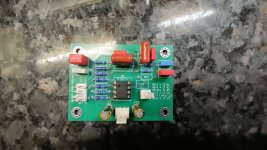
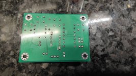
Here is the latest revised schematic and board layout. I dont expect folks to keep holding my hand but I add the new revision here for completeness.
Got rid of the series resistors and followed the schematic designations; adding a little footnote to the PCB for clarity. Added means to short the open input to gnd.
Practised with plotting to gerbers and I managed to upload to JLCPB without errors so im happy with that process.

Well spotted .I guess I'll be populating C13 backwards then!
And point taken RE the traces thru the ground plane..I guess I was avoiding top traces being directly under a component.
And point taken RE the traces thru the ground plane..I guess I was avoiding top traces being directly under a component.
Top traces can be under components. First off, because components are generally in some kind of plastic package. Secondly, because the board will have solder mask on top, so the copper is isolated from the components by a film.
You have acid traps on the sound end of R9 and the west end of R5. Acid traps are where copper meets at an acute angle. In the old days you'd get over-etching in those spots. Modern PCB processes are designed to avoid that, so traps aren't the issue they once were. It's still not a good practice to have traces come together at acute angles.
You could just flip C13 in the schematic. That error traces back to there.
I find your decision to use SMD capacitors for the bypass caps on the opamp a bit odd. What size are those? 0603? They'll be "fun" to solder by hand if you're much older than 40... 🙂
Tom
SMT decoupling caps are much lower inductance, and if you have any sense you use an oven to reflow SMT (such as converted sandwich toaster!). For example a mix of 0603, 0805 and SOIC:I find your decision to use SMD capacitors for the bypass caps on the opamp a bit odd. What size are those? 0603? They'll be "fun" to solder by hand if you're much older than 40... 🙂
Its all about using the right tools - be it magnifiers, non-magnetic tweezers, stencils, ovens - I took up SMT later in life, its not as scary as many think is my point...
Point taken about acid traps.
SMD caps local to opamp power pins because I'm fine with 0805 and even 0603 and I was advised to keep as close as possible.
Thanks again for the advice. Small run of boards coming along with a load of other stuff from JLC. Shall do some trialling.
SMD caps local to opamp power pins because I'm fine with 0805 and even 0603 and I was advised to keep as close as possible.
Thanks again for the advice. Small run of boards coming along with a load of other stuff from JLC. Shall do some trialling.
BTW you can't see the decoupling caps on my board above as they are mounted on the rear-side to be close to the IC pins without getting in the way of the signal routing... Another trick you can pull with SMT.
I got the boards in and have populated one for testing. I initially tested without the OP and proved good rails with my chosen PSU. (+/- 20v).
Leaving the input unconnected, would you expect to see approx 18vdc on the output pin (#7) of the opamp.?
I've followed a spreadsheet for the values I need for my chosen LT boost. I intend to get an audio engineer to plot the response for me until I learn how to do that. Initially I was going to feed it a signal and measure the AC output at say 500hz or somewhere well out of the LT range. And then lower the frequency being fed in and hopefully once I get to approx 50Hz I should start to see an appreciable increase in output voltage.
But at the moment this 18vdc on pin 7 has me wondering if there is a fault in my design!
Attachments

Op amp outputs should never have high DC voltages present. Perhaps just a few mV.
The second op amp appears to be running open loop at low frequencies and DC.
There must be a proper, controlled amount of DC gain to avoid integration to the rail.
Your earlier version did not have this problem.
The second op amp appears to be running open loop at low frequencies and DC.
There must be a proper, controlled amount of DC gain to avoid integration to the rail.
Your earlier version did not have this problem.
U1B has no feedback at DC so it'll amplify the DC offset from U1A by its open-loop gain. So, yeah... I'd expect it to rail. Bummer that this wasn't caught in the schematic review. You could fix this by shorting out C9.
Tom
Tom
Thanks guys. I laugh when reading those 2 replies as they literally mean nothing to me! But your comment on shorting C9 Tom, makes me see what you're both referring to.
I seem to have moved C9 in the schematic in the latter revision...I think I see the error of my ways.
I seem to have moved C9 in the schematic in the latter revision...I think I see the error of my ways.
- Home
- Design & Build
- Electronic Design
- Anyone care to critique my first Ki Cad project? - Linkwitz Transform