Amplifierguru: If you look closely at the 1000 uF at the top left part of the schematic, you will see it is a bootstrap, allowing the output to go the +Vs rail. The 1k2 is the pull up resistor. 😉
Another thing is the 4.7V zeners on the gates of the IRF's are too small. The IRF's can't turn on properly at heavy currents. Try with 12V instead.
Another thing is the 4.7V zeners on the gates of the IRF's are too small. The IRF's can't turn on properly at heavy currents. Try with 12V instead.
Lars Clausen said:Amplifierguru: If you look closely at the 1000 uF at the top left part of the schematic, you will see it is a bootstrap, allowing the output to go the +Vs rail. The 1k2 is the pull up resistor. 😉
Another thing is the 4.7V zeners on the gates of the IRF's are too small. The IRF's can't turn on properly at heavy currents. Try with 12V instead.
Ooops, you are right - wrong schematic version - they are supposed to be in series with 1N4148 for about 5.2V but the simulator drives me nuts with ideas about series connected diodes.
Actually, IRF150 will turn on adequately for a 4 Ohm load from a 36 rail (40V is indicated on the schematic but under actual load conditions, 4V droop is anticipated). It is after all a small sub 😉. Two things to keep in mind:
1) Zeners are dimensioned for >=50 degree operating temperature.
2( there are NO source resistors. normally, these would contribute a large voltage drop at peak current, and the zeners would have to be for a larger voltage, like you mention. 12V zeners on a IRF150 would mean in excess of 100A peak current on an IRF150...
amplifierguru said:posted reply on wrong thread, here it is -
Hi Ilimzn,
Sure I'll comment on your design. Firstly why pure Nch output? An exercise? The asymettry usually leads to high OL distortion and the symettrical complementary drive opportunity is lost.
The reason is to take oportuniy of easy rail to rail drive:
1) Bottom Nch is a prime candidate to be driven right into saturation, as _in_theory_ you have the whole rail-to-rail voltage to do it with.
2) A bootstrapped VAS also has the ability to swing past the top rail, which again, in theory, gives you the ability to saturate the top N ch transistor, this would be N ch for a complementary SF output as well.
The alternative would be something like a CFP output stage with gain, but as you yourself said in another tread, taming distortion and oscillation can be a problem. I actually have a design like thet and indeed it has higher distortion figures although intuitively, one would not expect it. Also, thermal stabilisation is a bit touchy as the servo element is actually in the front end... It also uses more parts, and at some point it became a challenge to use as few as possible 😉
Having said that, it appears to derive from the Bengt Ollsen design from EW&WW (Dec'94) "Better Audio from non-complements".
Seen the design but this one had nothing to do with it 🙂, in fact, I had Nelson Pass' MOS Citation 12 already captured for the simulator and sort of simplified it into this 😉 and added the necessary components to handle limit operating modes...
Why the 3K3 at input , you don't need it. Move the 560p to after the 1K - right to the input base. Bit more gain too (2.1dB).
Again a remenant of the actual usage - the 3k3 is a part of the driving electronics that I have no influence with. The capacitor is indeed connected to the base of the BJT - it's getting difficult to track all the intermediate versions of the thing 😉
The 10K on TR1 emitter isn't really clean sourced (your sim won't show that up unless you put some hash on the 40V supplies) and the 18pF probably won't matter for a sub amp.
Actually, it is sourced from the output and is part of the global feedback loop.
The IRF520 and associated resistors, as well as the 1000uF capacitor across it form a bootstrap current source for the VAS and doubles up as a Vgs multiplier bias voltage generator. This makes the voltage across the 1.5k and 10k series combination quite stable both in DC and AC terms, and very tightly tied to the output. Thus, both the 10k and the 1.5k form a feedback resistor, but their midpoint compensates for the Vbe drop of the input BJT alowing DC coupling. In the actual amp, there is a trim-pot there to trim out DC offset. Once this is done, it is surprisingly constant with temperature and supply voltage, for such a simple 'correction' - about +-150mV, which is completely acceptable for a subwoofer. Without coupling the bootstrap and bias functions together, it would not be possible to make the input reliably DC coupled.
The 18pF is not needed for normal operation, but it sorts out some oscillatory tendencies at overload and current limit. Similairly, a MOSFET VAS was chosen to avoid some storage problems with BJTs (again, keep overload and current limiting operation in mind - under normal circumstances this is a non-issue). A BJT VAS with a schottky guard against saturation on overload or current limit would probably be of benefit. At the time I designed this, i could not get 100V schottky diodes so I opted for a MOSFET instead.
Does it really get to the +Vs rail?
Hard to believe.
Yes, the bootstrap/Vbias generator takes care of that.
In order to be able to swing up all the way, a P ch MOSFET has to be used to drive the bottom IRFP150, and one with a high threshold voltage at that. This is because the bootstrap voltage equals Vbias, which is Vth of the IRFP150 + Vth of the IRFD9110. This voltage has to be enough to turn on the IRFP150 up to peak current or more, which also means the ability of the P ch MOS to saturate well without storage effects is crucial here. These two also form a sort of CFP by virtue of the P ch source being tied to the N ch drain through the bootstrap cap for AC.
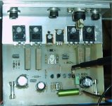
So, to get back to my amp, I did some more changes, putting a R at the Source of IRF9640, and now it seems to be totally stable. Attaching the schematic here and I will run 10kHz and take some pictures as amplifierguru wrote. I will also post pic of the amp
Thanks for all help!
Regards,
Bengt
Thanks for all help!
Regards,
Bengt
Attachments

Hello ilimzn I think Bengt is little bit angry with you, as you high jacked his thread, ilimzn not to be a thread jacker.😀 😀 😀 😀 😀 😉
Well, he has a right to be though I did not intend to thread-jack. Bengt, feel free to use any idea from my R-to-R amp you like... The reason i posted it is because it tries to solve the rail loss problem in a topology similar to yours. It could be easily adapted to your front end (in fact, it started with a front end very similar to yours). more on this below. I will also try to redeem myself by giving two suggestions about your amp:
1) Put a capacitor between the collectors of the BF469 and 470, a few tens of nF quality foil will be great there.
2) If you have a smaller Pch MOS than the 9640, you may want to use it instead. Something like a 9610, say. It has a much lower capacitance than the 9640, why let your VAS drive a higher capacitance if you can avoid it?
3) You may want to change the Vbe multiplier with a Vgs multiplier to generate the bias voltage. The one you now have in yur diagram will overcompensate the bias current, especially with the extra diode in series with the emitter.
Thankas for your reply and suggestions ilimzn. I am not angry  ..... It is good to se and discuss other constructions to solve problems. I did some changes to the amp as you can see on my last attached picture. When testing the amp seems to be stable at idle set to ~100mA. In my prototype I use doubble O/P (4 IRFP260).. I will put a cap between collectors of BF469/470 as suggested. And later post pictures of 10kHz sq wave.
Thanke !!
Bengt
..... It is good to se and discuss other constructions to solve problems. I did some changes to the amp as you can see on my last attached picture. When testing the amp seems to be stable at idle set to ~100mA. In my prototype I use doubble O/P (4 IRFP260).. I will put a cap between collectors of BF469/470 as suggested. And later post pictures of 10kHz sq wave.Thanke !!
Bengt
It took me too long to edit the above post so i am adding more notes below:
3) You may want to change the Vbe multiplier with a Vgs multiplier to generate the bias voltage. The one you now have in yur diagram will overcompensate the bias current, especially with the extra diode in series with the emitter.
4) Your VAS current is about 5-6mA, which is a bit too low for driving the relatively large gate capacitance of a IRFP250 and IRF9640. Look at suggestion 2) and also look into increasing the VAS current, I would go for double what you have as it is now, and perhaps even with the decreased capacitance resulting from the use of suggestion 2). You will need even more VAS current for multiple output devices!
I see two problems in your design:
You will have substantial rail losses, i.e. the output will not be able to swing very near the rail voltage, which means loss of potential output power and more heat on the output transistors. This in itself may not be a great concern, however, your design has unequal rail losses (much higher on the negative side), which means the amp will clip asymetrically.
The other problem is the overcompensating bias generator.
Here are some suggestions:
On the positive side, the driver can swing as high as one diode drop below the positive rail, assuming zero output current. Assuming say 40V rails and 8 ohm load, the total loss will then be that diode drop, plus VgsMOS + V on the 0R33 resistor. This will total about 7V or so. Vgs is the largest contributor, about 5V for the required output current. As the MOSFETs heat up, this will go down slightly as gm of the MOSFET increases.
On the negative side, things are, to my mind, not acceptable, two times (Vgs of the P250 + drop across the 0.33 ohm resistor) - two because the voltage bewteen P250 G and -V appears on both the 12 ohm resistors! Just this effect will be responsible for 10-11V of loss on the negative side. Net loss will be about double of that of the positive side. Using a smaller MOSFET from suggestion 2) above will not change this unless you use a MOS with a very high threshold (> Vgs of the 250 + voltage on 0R33).
Some suggestions:
You can make things better by increasing the bottom 12 ohm resistor and/or decreasing the top 12 ohm resistor. 100 for the bottom should be fine and will reduce the multiplying effect of the Vgs of the P250 plus voltage drop on 0R33. It will also decrease the amount of heat from the P-MOS. Watch the stability when lowering the 12 ohm in the source of the 9640, but better still, put a 100ohm damper resistor in series with the gate of the 9640!
Finally, you may be able to get better results if you use low threshold and higher gm MOSFETs as long as you keep gate capacitance low.
Alternatively, and perhaps obviously, use a PNP BJT. The latter, combined with careful choice of values for what are now the top and bottom 12 ohm resistors, can reduce the rai lloss to about the same as for the top rail, which is certainly a worthy goal. Keep in mind that if, what will then be, the emitter resistor of this BJT is reduced to very low values (removing it completely may be problematic for stability), this BJT will figure in the output stage's thermal stability, so the bias generator needs to be slightly different than for a pure VMOS design.
As for the bias generator:
A Vbe multiplier has a thermal gradient of 2mV/deg C times the multiplication factor of the Vbe. Since typical Vbe is 0.6V and typical threshold for MOSFETs is 2.5-3V, for two MOSFETs you need to generate bias voltage of about 5-6V. This means a multiplication factor of 8 to 10, so your thermal gradient becomes 16-20mV/deg C. VMOS typically has about 3mV/deg C gradient, so your 18-20 is grossly overcompensating even with no source resistors (the 0.33 ohm ones).
The 0.33 ohm resistors in your amp actually make the situation even worse as they lower the 3mV/C gradient even further. They also take away about 1.25V of clipping headroom, and reduce the already low gm of the MOSFETs. If you were using paralleled MOSFETs on the output, their use is mandatory, but for one pair, take them out.
That still leaves you with overcompensation due to Vbe multiplication being too big. You have two approaches you can use: either use a different sensing element, with lower thermal gradient or one that needs a lower multiplication factor, or reduce the multiplication.
The first approach is best done by using the same type element to sense temperature as the ones you are compensation - a MOSFET. The Vbe multiplier becomes a Vgs multiplier. The Rdg and Rgs will be approximately equal as the multiplication factor will be slightly less than 2. Since gm of a MOSFET is far lower than that of a BJT the capacitor from suggestion 1) above is mandatory or bias will be a function of the output voltage, which adds distortion. If the output stage uses a PNP BJT with a low value emitter resistor instead of the PMOS, you can use a 1N4007 in series with the drain of the Vgs multiplier MOS or even a small MOSFET with G and D connected together, in series with a diode, in series with a trim-pot, MOS needs to be on the heatsink, and the diode in thermal contact with the PNP BJT or at least close to it.
The second solution, which lowers the multiplication factor, and accomodates both a PMOS and PNP BJT output is a degenerated Vbe multiplier. Instead of the 1N4007 diode, put a small resistor, on the order of 10s of ohms. Start with a low value (10 ohms) and increase until you get good thermal tracking. The resistor will be about half for a PNP BJT used instead of a PMOS. The PMOS or PNP BJT would best be situated on the same heatsnk as the outputs in this case.
hope this helps!
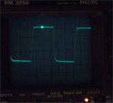
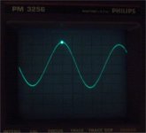
Bengt, ehat is the voltage scale on your scope pictures (V/cm)?
Also, what kind of load are you using?
Also, what kind of load are you using?
Hi Bengt,
The pics are better just a shade dark. See the top corner of the rising wave and compare with the bottom corner of the falling wave (rounded). It could peak up approaching clipping.
First you need to change the R =120 on the input stage current source to, say, 680 to lower the input stage current (excessive) and increase the gain. Then re-do the 10Khz square wave and post. Sinewave looks OK. If it's 10KHz take it to clipping and post.
Cheers.
- Status
- Not open for further replies.
- Home
- Amplifiers
- Solid State
- Another N-channel