But if the input change to noise common mode, the common mode rejection still very high.Fair enough. Though if the common mode noise rejection could easily, and inexpensively be made better by a minor circuit alteration that doesn't negatively affect the performance aspects you value, then it would sure be a shame to miss the opportunity.
Attachments

Hi Bimo,
This is why I posted. You did a great job. This circuit looks great. I expected the very nice nice common mode rejection with perfectly mathematically matched components. The front end looks very nicely balanced.
What worries me is what might happen when real world component tolerance gets considered, especially at the C2, C3 locations but everywhere in the balanced section, really. I have not simulated your cirrcuit so maybe it isn't as bad as I'm thinking.
Resistors are not so bad since you can buy low cost metal films @ 0.01% tolerance for not much extra money.
Capacitors are the worst with 1% tolerance being the best case scenario. Try the simulation again with C2 or C3 value changed by 1% to understand the motivation behind the That Semiconductor app note clip I posted in an earlier post.
I do not intend to be harsh. I only posted because I like your circuit and I thought maybe you would like my message after simulating it. I hope I'm not wrong.
Best regards,
Ugly
Edit: by the way, where is your cartridge model, brother? you gotta get that in there too, for trustworthy ac analyses.
Last edited:
since I am not allowed to edit my post above, ie apparently past the 30 minute time limit, I would like to point out a mistake.
I should have said C1 and C3 not C2 and C3 oops!
What's with that 30 minute rule anyway?
I should have said C1 and C3 not C2 and C3 oops!
What's with that 30 minute rule anyway?
I agree, because it is non global negative feedback, so almost all components need to be best as possible.
With global negative feedback, the important is the feedback components and the components outside the feedback loop because they cannot corrected.
With global negative feedback, the important is the feedback components and the components outside the feedback loop because they cannot corrected.
Why not placing a 22pF cap between the gates, that has the same impact as two 47pF caps to Gnd, but without spoiling CMRR and having the trouble to tightly match two caps.
Hans
Hans
Good idea. Thank you.Why not placing a 22pF cap between the gates, that has the same impact as two 47pF caps to Gnd, but without spoiling CMRR and having the trouble to tightly match two caps.
Hans
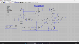
First stage is transconductance; voltage in, current out. Output current gets converted to voltage by the load. If load is resistive, you can change the resistor value to implement constant S/N ratio volume control (like Ayre does). If the load is an impedance, then you can do frequency-shaped gain, such as RIAA equalization as Bimo is doing. After the frequency shaping load impedance is a diamond buffer to do line driving. Depending on the values chosen for the RIAA shaping network, it "might" be nice to use a JFET buffer in front of the diamond. Overall this is a nice topology for a phono preamp.
I am not able to criticise you, and you are not in a position to teach me circuit design.
The usual RIAA network in said position has two R and two C and I was wondering why
Bino arrived at 6 R and 4 C. Even if you combine parallel parts this is no usual network.
The usual RIAA network in said position has two R and two C and I was wondering why
Bino arrived at 6 R and 4 C. Even if you combine parallel parts this is no usual network.
The output impedance of the first stage is not flat and not near zero, so I tweak the high frequency a bit until the frequency response is almost flat. The output impedance is around 117 Ohm at 1 kHz. If attenuate the output with a resistor that series with output impedance, The RIAA equalizer more easier. But I think this is not wise trade-off.I am not able to criticise you, and you are not in a position to teach me circuit design.
The usual RIAA network in said position has two R and two C and I was wondering why
Bino arrived at 6 R and 4 C. Even if you combine parallel parts this is no usual network.
Attachments
- Home
- Source & Line
- Analogue Source
- Another Idea of Balanced Moving Magnet Pre-amplifier