R14 with a nominal value of 250 kOhm in the collector circuit Q5 , eliminates the need for Q5 in the schemeAlmost there but the top..


Quite right Henk, with too large a value it seemed to neglect the effect of Q5. I have now reduced it to 4k7.R14 with a nominal value of 250 kOhm in the collector circuit Q5 , eliminates the need for Q5 in the scheme
I also found out that with R24 removed and by disconnecting the connection between Q5 emitter to minus rail and placing a resistor at Q5's emitter to minus rail makes the bottom of the square wave rounded. Just like the figure at post #60.
Also by increasing C3 compensation cap at VAS..makes the top of the square wave rounded however the opposite happens at the bottom, the squared corner comes back again...this effect is happening only at the higher frequency. I see no problem at 1KHz region.
I do not quite understand the purpose of such detections?I also found
C3 is a frequency shunt that combines the collectors of Q5 and Q2 into a Darlington assembly as the frequency increases, Walker was the author of this driver design. but later he himself abandoned such additional frequency non-linearity in the amplifier. Why repeat what was abandoned?Also by increasing C3 compensation cap at VAS..
All non-linearities that occur at a unity gain frequency of 1-10 MHz are directly related to a frequency of 1 kHz, this cannot be neglected ...this effect is happening only at the higher frequency. I see no problem at 1KHz region.
I am not aware of this as I am not a knowledgeable person about the application, I learned TPC here at DIYAudio.I do not quite understand the purpose of such detections?
C3 is a frequency shunt that combines the collectors of Q5 and Q2 into a Darlington assembly as the frequency increases, Walker was the author of this driver design. but later he himself abandoned such additional frequency non-linearity in the amplifier. Why repeat what was abandoned?
I am still in search of a better working scheme for the singleton design that is my purpose of 'such detections' because in the present status of the circuit, things does not seem to work well.
Albert
because in the present status of the circuit, things does not seem to work well.
Yes, that is right. why not repeat the finished one? to come up with your own, you need at least a year, tk. after assembly, debugging and test listening is necessary - do you have so much free time?
He he, yes I will. When I joined DIYAudio I was so enthusiastic that right away I built a number of circuits but I now refrain myself from doing that again. Perhaps I would say, I feel that the time to build for another amp is not right at the moment. I prefer to extend more time for simulation for now. But you'll never know, maybe tomorrow or the following day I will start working with the LTP IPS pcb lay-out. 🙂Yes, that is right. why not repeat the finished one? to come up with your own, you need at least a year, tk. after assembly, debugging and test listening is necessary - do you have so much free time?
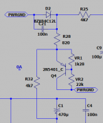
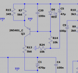
May I ask, what is the difference between these two current source configuration.
In the first case, these are two series L-shaped converters, the first is a stabilizer implemented on a zener diode, the second is an electronic potentiometer on a transistor with low differential resistance, so as not to use the capacitance.
The second option is a standard source of stable current, although it is implemented redundantly and, in fact, is not very true, since its internal resistance does not increase this way.
CS_A seems to favor singletons..but why..🤔
The first option can be physically used if the input stage has a low output impedance, or, simply speaking, an emitter follower. The second one is more universal and therefore used more often and it is more linear for the input circuit.
Thanks Henk,
I did not see much difference in simulation using each one on the singleton design, except that the first one (CS A) is very tricky to configure. R32 R28 R35 needs to come up with a fix value in order for VR1A to gradually respond into a step by step adjustment. The second one (CS B) is much easier to adjust via R15.
Do each one (or which of them) contribute to a better current regulation? I run a PSRR simulation of the circuit using both, the results were the same at 108dB.
Albert
In my opinion, the second option is better, because it does not use the ground as a reference point, which eliminates the additional current modulation of the reference voltage of small-current signals through the gnd track.Do each one (or which of them) contribute to a better current regulation? I run a PSRR simulation of the circuit using both, the results were the same at 108dB.
That is, R24 must be correctly connected to the opposite power rail.


- Home
- Amplifiers
- Solid State
- Another CFP output design attempt.