That sounds like something that'd happen to me, it's always just my luck with strange rare issues. haha It seems the more time and care I put into something the more likely it's to happen. Other times I slap things together with reckless abandon, and it's fine for years of service.Never saw anything like that.
Once I built a tube preamp, all new parts. Crackling noise in the phono stage.
After some irritation, the input plate resistor, a Dale metal film CMF55, was implicated.
I called the factory and had a discussion. Turns out someone handled the bare elements
with their hands before assembly. A whole lot were bad.
Another thing I thought it may have been at first was metal shavings from the self tapper screws used to hold the top lid of the amp chassis. Those screws are right above the gap of the PCB and heatsink. I can't really see back there, but I blew compressed air back there for days just in case.
Take it apart, gonna happen sooner or later.
Sheet metal screws don't belong in electronics, and never have.
Sheet metal screws don't belong in electronics, and never have.
I had very similar symptoms, when my clean ground wire was disconnected from the pcb (one channel only, 2nd channel was connected OK).
This created some strange ground loops.
On my PCB dirty ground and clean ground had separated wires going to the PSU..
I guess this case was an equivalent of missing ground-lifting resistor.
This created some strange ground loops.
On my PCB dirty ground and clean ground had separated wires going to the PSU..
I guess this case was an equivalent of missing ground-lifting resistor.
I was thinking grounding issues at first too, because the sound would fade when I touched certain spots with my finger. But both sides are connected the same way to the same point. It certainly acts grounding related, except for the fact that the noise can be made to come and go with my just blowing air across some transistors.I had very similar symptoms, when my clean ground wire was disconnected from the pcb (one channel only, 2nd channel was connected OK).
This created some strange ground loops.
On my PCB dirty ground and clean ground had separated wires going to the PSU..
I guess this case was an equivalent of missing ground-lifting resistor.
Not yet, no. I think I'm going to try a lab power supply while the board is still attached to the heatsink. I wouldn't be able to test anything once it's off the heatsink, can't apply power to it without the output transistors going into thermal nuclear meltdown. In order to take this thing apart I have to take the whole chassis apart to reach the screws that are keeping the heatsink in. Those film caps rarely fail, but it does seem like C1 may be a culprit due to the behavior of the circuit.any luck with narrowing it down to a specific area?
I am able to make the noise reappear by cooling the transistors near the bias circuit. When cooling near the input transistors there's little to no effect.
Update, I've got the channel in question hooked up to my lab power supply @ 30-0-30 VDC. I can't get it to make a peep... it's working as there's hum when I touch the input. 🤷♂️🤦♂️ Either it's because of the lower voltage, wiring issue, or power supply grounding issue?
Since the supply is shared, that should be ok. If it's an instability, the absolute DC supply voltage could
make a difference. If you have two of those supplies, series connect each chassis and try higher voltages.
Look at the board carefully, clean it and check soldering.
make a difference. If you have two of those supplies, series connect each chassis and try higher voltages.
Look at the board carefully, clean it and check soldering.
Last edited:
No additional power supplies. I shall check and clean the board, but not today. Had my dose of this for today. 😆 Thanks for the tips everybody!Since the supply is shared, that should be ok. If it's an instability, the absolute DC supply voltage could
make a difference. If you have two of those supplies, series connect each chassis and try higher voltages.
Look at the board carefully, clean it and check soldering.
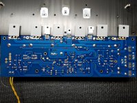
In the image shown in post 17 it appears the input ground goes nowhere (see 1 in attachment) floating on a make shift RCA socket there is no shielding - whereas the output lead (see 2) is quite close and the speaker earth wire which would normally be twisted together with this. Thirdly (see 3) the transformer wires to the bridge rectifier should also be twisted. To make a point of difference between your two channels - the bridge rectifier and where the protection pcb both lie these have to be closer to the channel with the noise problem with channel that is trouble free. I suggest you should look up member Bonsai's web pages to see how he avoids issues with layout and grounding.
Attachments
Mjona, thanks for the tips. My griunding could use some cleanup; but I think this issue is beyond ground wiring.
I was able to get the board off and tested c1. Measures bang on.
Checked my solder work, i think i did a good job. Attached a video and pics.
Solder Video
I'm leaning towards more of a bad semiconductor.
I was able to get the board off and tested c1. Measures bang on.
Checked my solder work, i think i did a good job. Attached a video and pics.
Solder Video
I'm leaning towards more of a bad semiconductor.
Attachments
In that case I would suspect D3 zener diodes produce noise and this one is part of the current mirror cascode section for the LTP. I notice that a number of components on this board are not soldered on the through hole rounds on the top face of the PCB and this one is a case in point. I cannot see D3 is soldered. under the board. The problem may be with D3 which appears to be correctly oriented from what I can see.Mjona, thanks for the tips. My griunding could use some cleanup; but I think this issue is beyond ground wiring.
I was able to get the board off and tested c1. Measures bang on.
Checked my solder work, i think i did a good job. Attached a video and pics.
Solder Video
I'm leaning towards more of a bad semiconductor.
Re your general layout the PCB is upside down and the toroid should be mounted with the leads on the top side and not against the side plate where these may be crushed by tightening the bolt. This can result in a breakage in one of the leads as have found out through experience and with regret.
There is a lot of emi about with capacitor bridge rectification charging pulses. The length of the wiring could be shortened by a different configuration of your various pieces of hardware. You could do that with the transformer rotating to a position where the wires leading to the bridge is more central to both amplifier modules.
Yes, it could be a bad via on the board. Make sure all pads with a trace on that side are soldered,
whether they are on the top or the bottom. Don't count on the via to make the connection.
whether they are on the top or the bottom. Don't count on the via to make the connection.
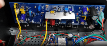
This is a pretty thick pcb. I used a lot of flux and higher heat on the iron. D3 is soldered well on both sides, just doesnt photograph well cuz the solder is very shiney and reflective. Either way i will test points on the board. Remember the issue happens when i cool certain transistors. Could be the long tail pair. I have time to test because i'm not really using this amp much. Using a 50 dollar chinese build that works perfectly with all protection circuits and preamp all on one board.
Use a piece of paper with a small hole to mask off the rest of the board when spraying a part,
to localize the problem better.
to localize the problem better.
I enlarged the image attached to post 31. I think it photographs well enough to show there are issues with the soldering.This is a pretty thick pcb. I used a lot of flux and higher heat on the iron. D3 is soldered well on both sides, just doesnt photograph well cuz the solder is very shiney and reflective. Either way i will test points on the board. Remember the issue happens when i cool certain transistors. Could be the long tail pair. I have time to test because i'm not really using this amp much. Using a 50 dollar chinese build that works perfectly with all protection circuits and preamp all on one board.
The solder would have enough flux in the mix so when a joint is preheated to melting temperature so when solder is applied it flows evenly onto the pad and lead so this sound electrically and mechanically. You have more control over this with iron temperature being correct, as it gives more time to observe and control the process than elevating the iron temperature.
If the preheating of the joint is left omitted and solder is heated and flowed over the whole there would be problems with the result.
I think something is unstable and is oscillating. Ive got the board out of the amp and when i heat/cool q7/q8 it throws things off. To a lesser entent q1/q2. On this channel i used heat shrink instead of a zip tie to couple them together like the good channel.
Q7/Q8 cold spray
Q7/Q8 cold spray
Post a circuit diagram - it is hard work tracking this down -the build thread is very long.I think something is unstable and is oscillating. Ive got the board out of the amp and when i heat/cool q7/q8 it throws things off. To a lesser entent q1/q2. On this channel i used heat shrink instead of a zip tie to couple them together like the good channel.
Q7/Q8 cold spray
There is a need to eliminate the possibility of an error with the input earth implementation. I alluded to this in an earlier post - the RCA jack hanging free in the chassis. Where does the tag connect to earth. Possibilities include through a low value resistor on the pcb - there is one sitting below the input screw terminal block - what value is this.
I didn't see any piece of paper with a small hole masking off everything other than the suspect transistors from saturation from the spray. How do you know it is unstable and oscillating what is your evidence. Does the dc offset change and do the output transistors get hotter than normal. You can test that by putting a finger on the body of one or more of these. The temperature on the small signal transistors should be low and not vary to any significant extent.
Thanks for your reply. I've had multiple rca jacks on the board. It is connected at the terminal block on the amp board. All grounding is done at the power supply. One ground wire from the board goes back to the power supply ground terminal. From or near that same point, the power supply is grounded to the chassis through a 10 ohm thermistor(CL-60). The speaker output grounds are also tied to the ground terminals on the psu, there is also one more ground from this point that goes to the speaker protection module as a ground reference for the circuit to detect DC offset on the output.Post a circuit diagram - it is hard work tracking this down -the build thread is very long.
There is a need to eliminate the possibility of an error with the input earth implementation. I alluded to this in an earlier post - the RCA jack hanging free in the chassis. Where does the tag connect to earth. Possibilities include through a low value resistor on the pcb - there is one sitting below the input screw terminal block - what value is this.
I didn't see any piece of paper with a small hole masking off everything other than the suspect transistors from saturation from the spray. How do you know it is unstable and oscillating what is your evidence. Does the dc offset change and do the output transistors get hotter than normal. You can test that by putting a finger on the body of one or more of these. The temperature on the small signal transistors should be low and not vary to any significant extent.
I don't have any proof of the circuit being unstable, other than the noise coming and going with cooling/heating of certain components. I did use the paper trick when testing just not for when I shot the video. It gave me the same results.
The output transistors don't seem to get hotter than usual, but I'm able to restart the noise by spraying the bias thermal coupling transistor on the main heatsink and spraying q7/q8 with cold.
Attachments
- Home
- Amplifiers
- Solid State
- Annoying Issue with HoneyBadger Amp