My old, beloved GW GOS-3310 has stumped me. It has been a faithful companion for years and then had an “event” that since has the amplitude variable as well as the vertical gain pot acting like vertical position, along with the actual vertical position control and DC balance pots.
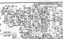
I have replaced every transistor, diode, and zener in the visible portion of the schematic pic below, and replaced or checked every resistor and cap. Voltages all good into the circuit starting with Q202, and good all the way to the CRT on the right with the notable exception that varying VR203 (amplitude) should increase Y1 and Y2 on the CRT equally and it doesn’t. VR202 (Gain) should do the same and it does not. VR201 and VR204 are DC balance, and all 4 of these move the trace vertically instead of changing the amplitude.
Anyone with higher schematic reading and troubleshooting skills than I might see what I am missing. Thanks in advance for any assistance.
I have a shiny new Rigol MSO5000 so I am not without a scope but I have a warm spot in my heart for this old single channel 10 Mhz scope.
Jeff
Attachments
If these have encoders, many scopes have reliability problems with those, including
HP/Agilent/Keysight, and LeCroy.
HP/Agilent/Keysight, and LeCroy.
Last edited:
Vr201 and VR204 should move the trace, that what DC balance does, however its to compensate for offset/leakage upstream. Id the amplitude/gain controls move the signal then there is significant offset going into those.
Check for DC at the gate of Q202 and the source of Q202. I suspect R213 is adjusted for setting the follower's dc offset at its output and changing the transistor would require a different value. What I would do is check the DC at the source of Q202, try to get it to zero with the input grounded. With that at zero then you can check the effects of the gain and DC trims. From your description the problem is at or just past the input stage.
Check for DC at the gate of Q202 and the source of Q202. I suspect R213 is adjusted for setting the follower's dc offset at its output and changing the transistor would require a different value. What I would do is check the DC at the source of Q202, try to get it to zero with the input grounded. With that at zero then you can check the effects of the gain and DC trims. From your description the problem is at or just past the input stage.
There is a troubleshooting trick at repairing oscilloscopes:
Short the collectors of Q207 and Q208 - the trace should jump to the center of the screen. Then move backwards: short the collectors of Q205 and Q206. If the trace jumps to the center then go one step further to the input, and short the collectors of Q203 and Q204 for a test. Shorting the collectors in a balanced amplifier is a safe operation (use insulated measuring wire though).
If all OK, the problem is in the input circuit. Check the voltage on the zeners. If they are OK, replace the Q202 FET.
Ok.
All tests done with source at ground.
There is indeed DC on both the gate and source of Q202. +6.20vdc on the gate and +1.36 on the source.
With the trace off the screen, shorting the collectors of Q207/208, 205/206 and 203/204 all bring the trace not exactly centered, one reticule below center in all cases. Q202 speced as a 2SK40C (unobtanium) has already been replaced with an NTE459, advertised as a direct replacement.
There is +9.5vdc at the right of R216 and exactly +6.2 as supplied by DZ201. C205, R210, 211, 212 and 216 all test correctly. There is -9.65vdc coming into R247.
Don’t give up on me yet!
Thanks,
Jeff
Attached is data on that odd transistor. Second from the bottom of the scan. It should be possible to match a suitable Jfet. My guess is that they used a particular sort (the C designation) for IDSS. The gate of Q202 should be the same voltage as the input and the output should also be about the same. Next step is to figure where the voltage on the gate is coming from. Also the pinout of the FET may be different from the errant part which could explain the odd voltage at the gate.
Attachments
More info
Thanks, Demian.
I should point out that the problem existed before I replaced anything. Unable to find a fault with a DVM and not yet having replaced the scope, I replaced all the semiconductors to no avail.
But in my poking around now for voltage, I have come across a portion of the schematic that I don’t understand. the pic below is the input stage.
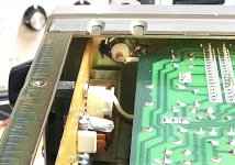
First, I don’t know what the dashed line between J201 and R 211 represents. The schematic shows the selector in GND. Looks to me then that J201 which is nothing more than two wires, one of which goes directly to ground and the other through S201 the selector, should have ground on both lines. It does not. In fact, throwing the switch between AC, GND and DC has no effect on the powered off status of either of J201 lines. It seems to me that with GND selected, the line to C220 and R211 should be grounded. It is not. I would blame the selector switch as being open, except the switch functions correctly best I can tell as I can get a signal trace on the scope both in AC and DC coupling, although it is near the top of the screen with full down position selected, and the variable has no effect. No adjustments of Gain, Position or Balance pots will get the trace centered, nor vary the gain.
The schematic also does not appear to show that the black lead from J201, the white connector in the picture, goes directly to the chassis ground and the white goes to the input BNC center connector. On the PCB the black lead goes to ground and the white lead goes to the selector switch. So it would appear that in one of the three switch positions, I would assume GND, the BNC center should be grounded through J201. But it does not. Lastly, I can’t tell where the VC arrays below the input section enter the circuit. Those are for horizontal calibration at different frequencies. I have not been able to calibrate with the variable problem so have not done any troubleshooting of those circuits.
The center post reads open on GND and AC, and 1Mohm on DC. Could the switch be bad or does this sound correct? Should the AC position also see 1Mohm? I get appropriate traces on both AC and DC, with the DC being offset vertically as it should.
Hope this sheds some light.
Thanks for your generous assistance.
Jeff
Thanks, Demian.
I should point out that the problem existed before I replaced anything. Unable to find a fault with a DVM and not yet having replaced the scope, I replaced all the semiconductors to no avail.
But in my poking around now for voltage, I have come across a portion of the schematic that I don’t understand. the pic below is the input stage.
First, I don’t know what the dashed line between J201 and R 211 represents. The schematic shows the selector in GND. Looks to me then that J201 which is nothing more than two wires, one of which goes directly to ground and the other through S201 the selector, should have ground on both lines. It does not. In fact, throwing the switch between AC, GND and DC has no effect on the powered off status of either of J201 lines. It seems to me that with GND selected, the line to C220 and R211 should be grounded. It is not. I would blame the selector switch as being open, except the switch functions correctly best I can tell as I can get a signal trace on the scope both in AC and DC coupling, although it is near the top of the screen with full down position selected, and the variable has no effect. No adjustments of Gain, Position or Balance pots will get the trace centered, nor vary the gain.
The schematic also does not appear to show that the black lead from J201, the white connector in the picture, goes directly to the chassis ground and the white goes to the input BNC center connector. On the PCB the black lead goes to ground and the white lead goes to the selector switch. So it would appear that in one of the three switch positions, I would assume GND, the BNC center should be grounded through J201. But it does not. Lastly, I can’t tell where the VC arrays below the input section enter the circuit. Those are for horizontal calibration at different frequencies. I have not been able to calibrate with the variable problem so have not done any troubleshooting of those circuits.
The center post reads open on GND and AC, and 1Mohm on DC. Could the switch be bad or does this sound correct? Should the AC position also see 1Mohm? I get appropriate traces on both AC and DC, with the DC being offset vertically as it should.
Hope this sheds some light.
Thanks for your generous assistance.
Jeff
Attachments
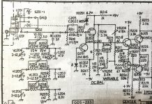
The dashed line indicates the two wafers of the attenuator switch are linked mechanically.
First test- DCR from BNC center to FET gate- should be 470K. Other end of R211 should be zero in DC. In AC should be open. A similar Tek input circuit is below, with essentially the same values for DC.
The BNC center should be 1 Meg to ground in all three positions or something bad could happen when connected to a power supply with a 1X probe. The Jfet input is grounded through the 470K resistor when grounded. The circuit looks correct although the drawing is not really clear. Its typical of Japanese schematics with the open circles for switch contacts.
Second Test- Look for a voltage drop across the 470K resistor in GND position. It should be zero.
The input when grounded should have zero V on the gate of the jfet. The bases of the first diff pair should both be about the same voltage.
Attachments
Measurements
DC R BNC center pin yo Q202 gate is open on AC and GND, 1M on DC. The 470K you mention is in series with a 470 ohm, but that still doesn’t add up to 1M. Exact same result for BNC center pin to chassis ground.
Q202 gate voltage is 0. My bad on the previous posts. Drain is 6.2 and source is 1.3.
Base voltages on Q203 and 204 are 1.43 and 1.21 respectively with the variable set to calibrate (full clockwise) and trace near center. Turning variable full counterclockwise takes trace off scope, Q203 and 204 are then 1.43 and 1.41, and Y+ is 27v and Y- is 154v explaining why the trace is no longer visible. Y+ and Y- voltages checkout with trace position. Trace is centered up when volts are equal and instead if varying them equally with vertical variable or gain adjustments, they diverge.
As difficult as it is, seems I need to remove the coupling switch as it does not appear to be providing the necessary ground. Baffles me how the trace when fed a signal seems to respond appropriately to that switch.
Thoughts?
Jeff
Switch checks out ok. Can’t explain lack of 1M resistance at AC and GND selector. Checked all attenuator R and C values since I could get to them. All good.
Don’t think there is a single input circuit component that hasn’t been checked and/or checked and replaced.
��
Jeff
Don’t think there is a single input circuit component that hasn’t been checked and/or checked and replaced.
��
Jeff
Hi Jeff,
Since you're observing Q202(input at GND) source voltage is 1.3V, I believe VR201 wiper should be adjusted to the same 1.3V Then there will be minimal shifting of the trace position when VR203 is varied. Then VR204 is adjusted to center the trace. At least that's what I believe should happen. Let us know how things behave if you follow this procedure.
Good luck!
Steve
Success
That worked, Steve.
I had a hunch all along it was a calibration issue since all the components checked out. But no matter how many times I tried to follow the calibration procedures in the manual I would get to a step that wouldn’t calibrate.
It’s not perfect, as the Gain control is now at max and is still a few mv short of correct amplitude but the variable is responding correctly and traces are nicely centered up. I think it needs a few more calibration routines since all the adjustments seem so interdependent.
I’ll probably see if I can match some of those diff pairs later but for now it is functional. I don’t have any idea why the 1M input impedance only shows up on DC. Perhaps that is normal?
Thanks to all who chimed in with the helpful advice.
Regards, and Happier New Year!
Jeff
Great news, Jeff! Congrats!
I assume VR205 is the gain calibration adjustment? Advise if you can't get satisfactory calibration.
If you're confirming input resistance with a multi-meter at the BNC input, it should be open circuit when AC coupled and 1M ohm when DC coupled for all input ranges.
Happy New Year!
Steve
I assume VR205 is the gain calibration adjustment? Advise if you can't get satisfactory calibration.
If you're confirming input resistance with a multi-meter at the BNC input, it should be open circuit when AC coupled and 1M ohm when DC coupled for all input ranges.
Happy New Year!
Steve
Gain
VR202 is the gain pot, and it is maxed out and vertical amplitude is just shy of where it should be measured by my digital scope and signal generator. I'd feel better if it were closer to midrange.
With Q202 source and VR201 wiper at precisely the same voltage, there is still slight vertical displacement with the Vert. variable, but it is usable.
The only other complaint is the trigger stabilization calibration procedure doesn't work. Instructions call for the temporary installation of a 330k resistor parallel with R343, at which point you are supposed to vary the stabilization pot until you just get a trace. There is no trace when the resistor is in place. But I am nitpicking. Trigger controls seem to work fine.
The horizontal calibration all works perfectly.
Besides the slightly low amplitude, the only vertical calibration I can't perform is the 50V/div. It calls for a 30-40v sine wave. My signal generator only goes to 10v.
Thanks again,
Jeff
Which high voltage are you referring to, Demian? And do you mean the slight deflection from the vert variable?
Demian has an interesting thought re HV influence.
I suggest tweaking VR201 to minimize trace shift re Vert variable. My earlier suggestion was partly to convey circuit concept.
I totally overlooked VR202. It appears that VR206 would also affect gain. What does your manual say about its function? Is there a link for a manual download?
To generate a larger test voltage, you might consider using an audio power amplifier to boost the output of your generator. Another thought is to use a suitable transformer to generate a 60 Hz sine wave from the mains.
Steve
Last edited:
I feel guilty having you guys spend so much time on my petty problem. Take some solace in that I am learning alot at your expense!
Matching the 201 wiper voltage with Q202 source DOES result in the minimum movement with v. variable.
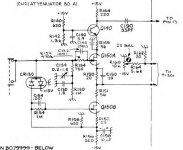
But it is interesting that you mention VR206 because it does influence gain and I never understood how since its only reference in the manual is for hf compensation. It is used only to flatten the tops and bottoms of square waves for each of the time/div settings.
I will attach the manual in pdf in the next post.
Jeff
Matching the 201 wiper voltage with Q202 source DOES result in the minimum movement with v. variable.
But it is interesting that you mention VR206 because it does influence gain and I never understood how since its only reference in the manual is for hf compensation. It is used only to flatten the tops and bottoms of square waves for each of the time/div settings.
I will attach the manual in pdf in the next post.
Jeff
- Home
- Design & Build
- Equipment & Tools
- Analog scope troubles