I was recently re-reading a thread about the maximum input levels for the 2x4 and hatched the idea for a circuit that would perform the following:
I have designed a circuit that does all the above quite nicely, with a pretty clean clipping and indication threshold. The limiting is performed by a biased shunt diode (or LED) on an op-amp buffer. The clipping detection circuit monitors the voltage drop on resistor in series with the input and detects the limiting action. I borrowed Rod Elliot's "pulse stretching" idea from his project 23 for a power amp clipping indicator. This makes sure that even a brief clipping incident will light the indicator LED long enough to be seen.
Clipping is currently not 100% hard, so you can still overdrive the input if you REALLY try. Hopefully the user will see the clip LED light and will back off on the source component level. I could configure a couple of ideal diodes to provide a 100% hard ceiling, or provide variable hardness via a pot.
Since it's very possible to overdrive the analog inputs of the 2x4 I thought that owners might be interested in this effort. I will post additional details shortly.
- Below the input voltage setting (0.9V or 2V), do nothing.
- When the instantaneous voltage reaches the maximum allowable input voltage, do hard limiting on the input signal
- When limiting action is present, light an LED in an obvious manner
I have designed a circuit that does all the above quite nicely, with a pretty clean clipping and indication threshold. The limiting is performed by a biased shunt diode (or LED) on an op-amp buffer. The clipping detection circuit monitors the voltage drop on resistor in series with the input and detects the limiting action. I borrowed Rod Elliot's "pulse stretching" idea from his project 23 for a power amp clipping indicator. This makes sure that even a brief clipping incident will light the indicator LED long enough to be seen.
Clipping is currently not 100% hard, so you can still overdrive the input if you REALLY try. Hopefully the user will see the clip LED light and will back off on the source component level. I could configure a couple of ideal diodes to provide a 100% hard ceiling, or provide variable hardness via a pot.
Since it's very possible to overdrive the analog inputs of the 2x4 I thought that owners might be interested in this effort. I will post additional details shortly.
Attached are pics of the functional blocks of this circuit from a simulator software.
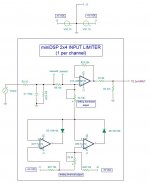
INPUT LIMITER:
This block performs the limiting action. The input is from a source component like a preamp and the output is connected to the input of the 2x4. There is an RF filter (R3 and C1) and R23 sets the input impedance. R9 and P3 set the input shunt. In normal operation there is no current flow through P3. R24 balances the impedance to the op-amp, minimizing DC offset (its in the tens of microvolts).
The limiting threshold adjustment potentiometer (P2) simultaneously sets a positive and negative limiting theshold bias voltage that is applied to ideal diodes formed by diodes D5 and D6 in the feedback loop of the op amps. P2 can be adjusted for the 0.9Vrms, 2Vrms, or any other threshold for limiting that the user desires.
When the instantaneous voltage exceeds the bias voltage on the ideal diodes they will conduct current away from the U1A op-amp input thought P3. P3 and R9 form a voltage divider. As the setting on P3 is adjusted to 0 ohms the limiting action becomes infinitely "hard", that is voltage is clipped at the limit setpoint. As the setting on P3 is increased the limiting action becomes softer and some overvoltage is allowed. Hard clipping provides the greatest protection from over voltage but produces the most distortion when activated. Soft clipping allows some over voltage but reduces distortion when activated.
In the absence of the clipping/limiting action the branch leading to the idea diodes is essentially out of the circuit and distortion will be very low. There is a small voltage drop ( a few percent) because of the circuit resistances under normal operation.
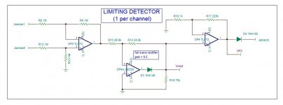
LIMITING DETECTOR:
In the presence of clipping/limiting there a voltage drop will develop across R9 in the input limiter block as current is drained through the shunt. This is sensed by the high impedance differential amplifier in the limiting detector block. This is actively rectified and then amplified. Output is via a diode.
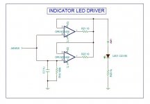
INDICATOR LED DRIVER:
The output of the limiting detector feeds an RC filter and buffers that drive the indicator LED. The action of the RC filter, combined with the fact that the output from the limiting detector is via a diode, causes the LED to light immediately but to dim slowly such that even brief clipping results in visible LED lighting.
Multiple limiting detector blocks can be connected to the indicator LED driver block, each through their own diode. As a result a single diode can show clipping for any number of channels (typically two inputs).
Thoughts and musings:
I cobbled together this circuit from circuits published by others and from circuits that I have developed for my own use. It uses lots of op amps, but all can be inexpensive types (the LME49740 could be a 5532). Simulated dynamic performance is good, and the circuit is adjustable.
If it was so desired, one of the op-amps in the indicator LED driver circuit could be used to drive an LDR placed in parallel with the 47k input impedance resistor. This would provide attenuation when clipping is detected instead of just effecting the extremes of the waveform. This may or may not be desirable, but it would be an easy addition to make to the circuit.
The limiter was originally envisioned for the input to the miniDSP 2x4 but it could be used for any limiting purpose of line-level signals.
INPUT LIMITER:
This block performs the limiting action. The input is from a source component like a preamp and the output is connected to the input of the 2x4. There is an RF filter (R3 and C1) and R23 sets the input impedance. R9 and P3 set the input shunt. In normal operation there is no current flow through P3. R24 balances the impedance to the op-amp, minimizing DC offset (its in the tens of microvolts).
The limiting threshold adjustment potentiometer (P2) simultaneously sets a positive and negative limiting theshold bias voltage that is applied to ideal diodes formed by diodes D5 and D6 in the feedback loop of the op amps. P2 can be adjusted for the 0.9Vrms, 2Vrms, or any other threshold for limiting that the user desires.
When the instantaneous voltage exceeds the bias voltage on the ideal diodes they will conduct current away from the U1A op-amp input thought P3. P3 and R9 form a voltage divider. As the setting on P3 is adjusted to 0 ohms the limiting action becomes infinitely "hard", that is voltage is clipped at the limit setpoint. As the setting on P3 is increased the limiting action becomes softer and some overvoltage is allowed. Hard clipping provides the greatest protection from over voltage but produces the most distortion when activated. Soft clipping allows some over voltage but reduces distortion when activated.
In the absence of the clipping/limiting action the branch leading to the idea diodes is essentially out of the circuit and distortion will be very low. There is a small voltage drop ( a few percent) because of the circuit resistances under normal operation.
LIMITING DETECTOR:
In the presence of clipping/limiting there a voltage drop will develop across R9 in the input limiter block as current is drained through the shunt. This is sensed by the high impedance differential amplifier in the limiting detector block. This is actively rectified and then amplified. Output is via a diode.
INDICATOR LED DRIVER:
The output of the limiting detector feeds an RC filter and buffers that drive the indicator LED. The action of the RC filter, combined with the fact that the output from the limiting detector is via a diode, causes the LED to light immediately but to dim slowly such that even brief clipping results in visible LED lighting.
Multiple limiting detector blocks can be connected to the indicator LED driver block, each through their own diode. As a result a single diode can show clipping for any number of channels (typically two inputs).
Thoughts and musings:
I cobbled together this circuit from circuits published by others and from circuits that I have developed for my own use. It uses lots of op amps, but all can be inexpensive types (the LME49740 could be a 5532). Simulated dynamic performance is good, and the circuit is adjustable.
If it was so desired, one of the op-amps in the indicator LED driver circuit could be used to drive an LDR placed in parallel with the 47k input impedance resistor. This would provide attenuation when clipping is detected instead of just effecting the extremes of the waveform. This may or may not be desirable, but it would be an easy addition to make to the circuit.
The limiter was originally envisioned for the input to the miniDSP 2x4 but it could be used for any limiting purpose of line-level signals.
Attachments
After some more simulation and tweaking of the circuit the performance is looking great. I added an input buffer before the op-amp that is doing the limiting to the audio signal. Since this circuit is an input stage, you need DC blocking (most important), and RF rejection, and cable termination, etc. The DC blocking is important because the presence of DC will cause the limiter to act asymmetrically, and that will introduce additional distortion. Also, the additional buffering will be useful if the LDR attenuator option is used in addition to limiting as part of the management of an overdriven input level.
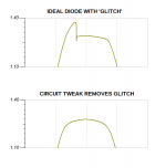
On thing that I spent a lot of time on was a "glitch" in the limiting behavior. It was very obvious for higher frequency (e.g. above 1kHz) sine wave inputs. This behavior is shown for a 5kHz sine wave input with modest overvoltage in the attached plot. I managed to figure out that this had nothing to do with the diodes in the ideal diode circuit but rather the fact that the op-amps used to implement the circuit were saturating at one rail when the ideal diode was not doing anything, and it took a little time for them to recover before acting normally. After some tweaks I have eliminated this behavior and the limiting action is now completely "glitchless". That's a great relief because the glitch would have added a huge amount of undesirable high frequency content and distortion.
I may design a PCB layout for this circuit. I think it adds some protection and functionality to the analog inputs for the 2x4, which is a pretty good DSP crossover unit for the money. The addition of the LDR would make a "compressor" type action possible, depending on the exact implementation scheme.
Attachments
I thought I would post little more follow up on what I did to fix the "glitch".... maybe someone can chime in on what is going on with the op-amps?
Initially I thought it was due to the op-amp saturating at one rail while the diode cut off the feedback. This doesn't seem to be the case. The voltage at the ideal diode op-amp's output DOES shoot up to the rail voltage, however, if I reduce the rail voltage the glitch remains. In fact the glitch is there even when I bring the rail voltage all the way down to the minimum recommended Vcc of +/-2.5V. But when I decrease the rail voltage just a little bit further, the glitch goes away. With continued reduced rail voltages the op-amp is not quite working properly although the input voltage is not exceeding the rail voltages at least - it can't because of the clipping action. So there seems to be a narrow "sweet spot". But this is in my simulator, not with a real device in the real world. Is this a behavior that I can depend on? What is happening when I reduce the rail voltage below the "minimum recommended" voltage?
Initially I thought it was due to the op-amp saturating at one rail while the diode cut off the feedback. This doesn't seem to be the case. The voltage at the ideal diode op-amp's output DOES shoot up to the rail voltage, however, if I reduce the rail voltage the glitch remains. In fact the glitch is there even when I bring the rail voltage all the way down to the minimum recommended Vcc of +/-2.5V. But when I decrease the rail voltage just a little bit further, the glitch goes away. With continued reduced rail voltages the op-amp is not quite working properly although the input voltage is not exceeding the rail voltages at least - it can't because of the clipping action. So there seems to be a narrow "sweet spot". But this is in my simulator, not with a real device in the real world. Is this a behavior that I can depend on? What is happening when I reduce the rail voltage below the "minimum recommended" voltage?
Update on more circuit tweaks...
I decided that the only way to get rid of the "glitch" reported above was to get rid of the op-amps creating the "ideal" diodes. I had used these because I discovered that a biased diode could not provide hard limiting with the circuit impedances I was using and, as the input signal level increased, the limited peak maximum would also continue to increase. Eventually the voltage would be able to overdrive the ADC input.
The solution was to fall back on the simpler concept of voltage biased diodes to provide soft limiting. A different way to hard limit the signal was needed and I turned to a rail-to-rail op-amp for this purpose. I found a unique op-amp that can provide clipping of signals that exceed the rail voltages while providing low distortion.
With these changes there is now well controlled and adjustable limiting AND clipping action. The diodes provide limiting with adjustable hardness and voltage threshold (e.g. you can do some compression). The rail-to-rail op-amp hard clips the signal just as the voltage reaches the ADC input maximum, and the device specs make it suitable for either the 0.9Vrms or 2Vrms input voltage option of the 2x4.
With this circuit, the user can eliminate digital clipping and control how the voltage of the input signal to the 2x4 is restricted. At the same time the input is given an RF filter, some ground loop rejection, a Zobel network to match the input cable impedance, and DC blocking with a corner frequency below 1Hz. All of this using low distortion active devices.
I continued working on the project yesterday. The improved circuit does the following:
Adjustable Compression / Limiting
--> onset can be set in 'dB below max level'
--> hardness / slope adjustment to vary between compression and limiting behavior
--> "glitchless" action
Output Voltage Limiting / Clipping
--> adjustable maximum output "ceiling" voltage
--> signal is symmetrically clipped with 100% hardness at the ceiling
--> clipping action can trigger AGC type gain reduction
Indicator LEDs
--> separate indicator LEDs for compression and clipping action
--> clipping action uses "pulse stretching" to increase visibility
This now has some nice user features that pair nicely with the miniDSP 2x4 and which are not available via the DSP software.
Charlie, do you have any interest in moving to Hong Kong? You could join the Dev Team and help add features to the MiniDSP lineup! Those guys could use a few more hands to get more of the features people want integrated and ready to ship.
Charlie, while ago I had trouble with minidsp overloading the input. I worked on clipping indicators, and I found simple circuits to work just fine...just for your information, check out the end of this thread.
http://www.diyaudio.com/forums/minidsp/230470-signal-level-minidsp-x-over-7.html
I dismantled system with minidsp since then, had to downsize, so it is not used at the moment. But one day I will use it again with those clipping indicators, they were fun to watch.
http://www.diyaudio.com/forums/minidsp/230470-signal-level-minidsp-x-over-7.html
I dismantled system with minidsp since then, had to downsize, so it is not used at the moment. But one day I will use it again with those clipping indicators, they were fun to watch.
Charlie, do you have any interest in moving to Hong Kong? You could join the Dev Team and help add features to the MiniDSP lineup! Those guys could use a few more hands to get more of the features people want integrated and ready to ship.
If they are interested in humoring me by picking up some of my ideas or designs I would be more than happy to talk with Tony about it. My wife probably wouldn't be too receptive to the idea of me moving to HK, however.
- Status
- Not open for further replies.