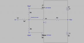
Negative feedback from a device's [for example a MOSFET] current-sourcing output [drain] to its summing input junction [gate] modifies its pentode-like electrical characterists to those like a triode. This is a neat and well known phenomenon. Such a MOSFET has been called a fake SIT [wrenchone], simulated SIT [Rothacher], etc. This means that a voltage variable current source [MOSFET=pentode] was converted to a voltage variable power resistor like a SIT which is likened to a solid state triode.
The attached concept schematic is originally a Pass DEF amp which was modified to utilize and exemplify this negative feedback. Its attributes are:
1. The FETs operate in the common source configuration. They provide voltage gain. The joint of their opposed drains is the current sourcing power output.
2. Negative feedback from the joined drains [out] is returned to the joined gates. The input and feedback signals meet at the joined gates which is a summing input junction.
It follows that the parent pentode-like electrical characteristic of both FETs prior to the application of negative feedback are simultaneously modified to triode-like. These FETs are now simulated/fake SITs.
I call this schematic a concept amp. But I have been listening to an actual prototype of a relative amp which demonstrated feasibility. I will report on its full schematic and performance. Here are its working FETs.
1. Replace SJDP120R085 in this schematic with IRFP140N N-channel MOSFET. Use +Vgs1.
2. Replace IRFP9240N in this schematic with SJ28 true SIT. Use +Vgs2
Its follows that the N-MOSFET [IRFP140N] became an enhancement fake SIT working with a real P-channel SIT [SJ28]. It seems to me that two birds of similar feather [a fake SIT with a real SIT] working together is more palatable musically than a pentode-triode couple.
Attachments
When I did the DEF amp, one of the things I also developed was a version
with my SIT-1 (N channel).
I call it the DEFaSIT.
😀
with my SIT-1 (N channel).
I call it the DEFaSIT.
😀
I call this schematic a concept amp. But I have been listening to an actual prototype of a relative amp which demonstrated feasibility. I will report on its full schematic and performance. Here are its working FETs.
1. Replace SJDP120R085 in this schematic with IRFP140N N-channel MOSFET. Use +Vgs1.
2. Replace IRFP9240N in this schematic with SJ28 true SIT. Use +Vgs2
Its follows that the N-MOSFET [IRFP140N] became an enhancement fake SIT working with a real P-channel SIT [SJ28]. It seems to me that two birds of similar feather [a fake SIT with a real SIT] working together is more palatable musically than a pentode-triode couple.
Interesting amp's projects i am curious about audio performances 🙂
When I did the DEF amp, one of the things I also developed was a version
with my SIT-1 (N channel).
I call it the DEFaSIT.
😀
Hobby amateur get few vintage sit's
 Semiconductors
Could nos 2SK180 sit vertical jfet with hockey puck IXYS can work in DEF stage ( cascoding ) ?
Attachments
When I did the DEF amp, one of the things I also developed was a version
with my SIT-1 (N channel).
I call it the DEFaSIT.
😀
Hello Mr. Pass. A befitting name. DEFaSIT clearly identifies this useful combination of FETs [with SIT-1] in their DEF. In your DEF thread, you had posted that you were playing music with/through it, and the sound of it was very pleasant. I fully agree. Still there is yet another surprise. Please convert your DEFaSIT [a DEF buffer application] to the scheme I showed above [not DEF] and enjoy yet another new signature sound which surprised me.
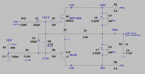
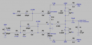
The attached schematic belongs to the amp under subjective study. Please note the following:
1. The FET couple [2SJ28/IRFP140N] and theiir biasing components to the left of their gates are those for a standard Pass DEF amp.
2. The two FETs are operating in push-pull common [grounded] sources, instead of push-pull common drains which is a Pass DEF [F=follower or buffer].
3. This FET output stage has voltage gain. Negative feedback from Vout to their gates gave a closed loop gain of ~ 3.6K/0.68K.
4. This negative feedback is likened to that of Schade Feedback. Consequently, it modified the pentode-like characteristics of IRFP140N; N-channel MOSFET to that with triode-like properties. The resultant MOSFET is a fake or simulted SIT with characteristics like those of a genuine SIT namely a voltage variable power resistor.
5. A Zobel in this amp is a must to delete a high frequency oscillation.
6. Idle current is rock-stable.
7. DC offset at Vout is also highly stable at~<10 mV. This resulted from the amp behaving like a DC servo.
7. The values and quality of the PSU filter caps are important because they pass output signal to the loudspeaker.
8. The PSU floats. Thus two psus are needed for a stereo amp.
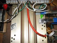
A pic of the FETs on the heat sink is attached. Soundhappy: I'll listen to it for a couple more days, and report fully before I replace these FETs with R085/IRFP9140N P-MOSFET. Todate, its sound is superb, highly detailed, and has its unique musicality which may well be the expecteted " overall SIT'ish".
1. The FET couple [2SJ28/IRFP140N] and theiir biasing components to the left of their gates are those for a standard Pass DEF amp.
2. The two FETs are operating in push-pull common [grounded] sources, instead of push-pull common drains which is a Pass DEF [F=follower or buffer].
3. This FET output stage has voltage gain. Negative feedback from Vout to their gates gave a closed loop gain of ~ 3.6K/0.68K.
4. This negative feedback is likened to that of Schade Feedback. Consequently, it modified the pentode-like characteristics of IRFP140N; N-channel MOSFET to that with triode-like properties. The resultant MOSFET is a fake or simulted SIT with characteristics like those of a genuine SIT namely a voltage variable power resistor.
5. A Zobel in this amp is a must to delete a high frequency oscillation.
6. Idle current is rock-stable.
7. DC offset at Vout is also highly stable at~<10 mV. This resulted from the amp behaving like a DC servo.
7. The values and quality of the PSU filter caps are important because they pass output signal to the loudspeaker.
8. The PSU floats. Thus two psus are needed for a stereo amp.
A pic of the FETs on the heat sink is attached. Soundhappy: I'll listen to it for a couple more days, and report fully before I replace these FETs with R085/IRFP9140N P-MOSFET. Todate, its sound is superb, highly detailed, and has its unique musicality which may well be the expecteted " overall SIT'ish".
Attachments
The attached schematic belongs to the amp under subjective study....
Soundhappy: I'll listen to it for a couple more days, and report fully before I replace these FETs with R085/IRFP9140N P-MOSFET.
Todate, its sound is superb, highly detailed, and has its unique musicality which may well be the expecteted " overall SIT'ish".
Yes Antoinel write more about your tweeks and experiments and what best sound quality options with actual configuration.
Greetings 😉
Attachments
When I did the DEF amp, one of the things I also developed was a version
with my SIT-1 (N channel).
I call it the DEFaSIT.
😀
Will we get a peek at this one? 🙂
You know I won't be able to resist. I have saved a small qty of the Sony
parts for the occasion.
parts for the occasion.
The attached schematic is for another power amp using simulated/fake SITs. It operates like that I described in an earlier post. Please note the following:
1. It is a derivative or an extension of DEF; meaning it has votage gain and Schade negative feedback so as to make in situ fake SITs.
2. The DEF FETs used in it are SJDPI20R085 and IRFP9140N. Both FETs are believed to become voltage variable power resistors post the application of Schade feedback.
3. A 0.1 Ohm degeneration resistor was used at the source of R085 to stop a slow upward drift of its drain current at idle conditions.
This is a great-sounding amp. It has a unique musical signature which most probably has contributions from its newborn fake SITs.
Attachments
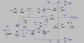
The 2 FETs in DEF and its derivative circuits have this sustained property or rule. The depletion FET; e.g. SJDP120R085 or other alway has a Vgs which is more negative in value than the Vgs of its P-MOSFET companion e.g. IRFP9140N. For example the schematic in the previous post showed Vgs = -4.16 V for R085 and Vgs = -3.74 V for IRFP9140N; both measured under the same conditions of Vds = /23V/ and drain current = /1.3A/. Other examples of this apparent rule are also found in the thread which is entitled "DEF" by Mr. Pass.
I "broke" this apparent rule in another fleeting prototype amp which uses simulated SITs. The P-MOSFET IRFP9140N was compounded with PNP [2N5415] in a Darlington-like device. This compound device essentially simulated or made the equivalent P-MOSFET which now has a Vgs = -4.35 V, versus a Vgs = -4.14 V for its companion R085. Why bother simulate this case? A pair of randomly selected FETs may by chance fit this status. A solution is present.
The schematic of this protype amp is attached. Please note:
1. The Schade feedback resistor [wrong value shown! should be ~3.7K] goes to R085 first and its continuing biasing string of resistors [to -23 V] then goes to the PNP-MOSFET compound. This biasing scheme is opposite to that where the FETs obey the intrinsic rule.
This is a great sounding amp. It is thermally stable; meaning it has a rock-steady drain current and an output DC offset of <50 mV.
Attachments
I think I showed a circuit (without the PNP device) which accomplished
the adjustment by attaching your R8 from Gate to Source and using the
voltage division with R14 and R8 to give the drop you want.
The most general solution is a pot across the Gates with the wiper attached
to the output.
the adjustment by attaching your R8 from Gate to Source and using the
voltage division with R14 and R8 to give the drop you want.
The most general solution is a pot across the Gates with the wiper attached
to the output.
I think I showed a circuit (without the PNP device) which accomplished
the adjustment by attaching your R8 from Gate to Source and using the
voltage division with R14 and R8 to give the drop you want.
The most general solution is a pot across the Gates with the wiper attached
to the output.
Thank you Mr. Pass for your reply.
I continue to use your method of voltage division to generate the appropriate Vgs values [any combination] for the FETs in DEF circuits. It is simple and highly reliable. I think that you meant R4 instead of R14 with R8 to generate Vgs values by voltage division.
The Vbe of PNP [0.6 V] was used to level shift the intrinsic Vgs of MOSFET from [~-3.7 V] to the still lower value of Vgs = -4.3 V for another unusual MOSFET. Thus I got the new and maybe rare Vgs combination of -4.14 V for R085, and -4.35 V for the simulated MOSFET.
The general solution of using a pot to generate appropriate Vgs values is also a simple approach. It may lack the flexibility of fine tuning the idle drain current. I think that you meant the wiper of the pot goes to the gate of one FET, one of its live ends goes to Vout and its other live end goes to the gate of the other FET.
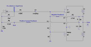
Amp with Simulated SITs plus Posistive Current Feedback
The attached schematic is a simplified version of that shown in post #14. I have also added the phase inverting operational line amp [U1] which drives the power stage. It shows the standard or formal application of Positive Current Feedback [PCF] inside it. Here' s a description of operation:
1. The output current passing through the 8 Ohm loudspeaker load is sampled as a voltage drop across the 0.5 Ohm in series with it. This voltage drop is Vpcf.
2. The music Vin and Vpcf are in phase. They are summed and amplified in U1 to get the indicated input signal to the power stage. [call it Vnet]
3. The ratio of amplified Vpcf to Vnet is calculated, normalized to 1 and converted to dBs.
4. I get 2-3 dB PCF boost with the indicated resistor values around U1. The magnitude of this add-on increased with decreasing frequency when using the loudspeaker below 100 Hz.
This amp and the loudspeaker sang marvelous music. This system is accurate. The ingredients of the music are highly resolved or become stand-alone entities. The time lapse between the attack and decay of instruments and vocals was minimized. These subjectives emanate from the expected increase in the amp's damping factor due to PCF. This amp and the ADS-L730 loudspeaker are working better together.
This PCF approach is fully useable in the schematics of past posts like #13 which is simpler to implement than that of #14.
Attachments
- Status
- Not open for further replies.
- Home
- Amplifiers
- Pass Labs
- Amps with simulated/fake SITs