Hi Bogdan,
I like the novelty of your design. By my reckoning your design has no single VAS stage but instead has two separate VAS stages formed by Q7+Q9 and Q8+Q10.
One issue with it is that if the two VAS stages do not behave in a perfectly complementary way then their outputs will "fight" and you will see cross conduction. It is as if you have designed two voltage amplifiers and then put them in parallel. To make them behave in a truely complementary way will be extremely difficult.
bogdan_borko said:Whot do you think about this design of mine.
It has no VAS stage, working in class AB.
(just simulation for now)
IS there any other design without vas and do you have the schematic?
This type of so called Current Feedback Amplifiers can be very fast.
Can easily get into oscillation, if not proper care is taken to avoid this.
Another issue is to try to get the idle current at correct and stable level.
Usually the compensation cap is not put across the feedback resistor
for this type of amplifier ( Emitter Feedback Amps is a better name ).
Instead, in your circuit should be a cap across R5+R10 and R6+R11
or alternatively from Q5 emitter to V+ and Q6 emitter and V-.
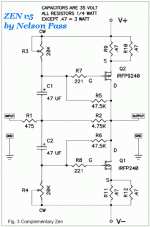
ZEN v5 .. Complementary ZEN
.
Sure there are several other Amplifiers
that uses the output complementary pair to do the voltage amplification.
Your circuit has one input stage + one VAS output stage.
In reality it is not the VAS you have removed
it is the last output stage .. the Follower you have removed!
Because in your circuit the VAS is the final stage .. but using slower more powerful output transistors.
")
There is a clever and interesting old boy in Texas USA
that has made a lot of different amplifier experiments.
One such try out is: ZEN v5 ... The Complementary ZEN
Before he had mostly used only Single End N-MOSFET output stages.
This time he investigated Push Pull.
Zen v5 takes your way to remove one stage .. a step further:
Nelson has here removed even the input stage!
Leaving us with ONE Powerful VAS stage
that acts also as input and output stage.
Links:
Papa! I want to have Zen V5
Pass D.I.Y. Amplifiers
Attachment shows the most beautiful and unique amplifier schematic
.. one of a kind ...
lineup
.
Sure there are several other Amplifiers
that uses the output complementary pair to do the voltage amplification.
Your circuit has one input stage + one VAS output stage.
In reality it is not the VAS you have removed
it is the last output stage .. the Follower you have removed!
Because in your circuit the VAS is the final stage .. but using slower more powerful output transistors.
There is a clever and interesting old boy in Texas USA
that has made a lot of different amplifier experiments.
One such try out is: ZEN v5 ... The Complementary ZEN
Before he had mostly used only Single End N-MOSFET output stages.
This time he investigated Push Pull.
Zen v5 takes your way to remove one stage .. a step further:
Nelson has here removed even the input stage!
Leaving us with ONE Powerful VAS stage
that acts also as input and output stage.
Links:
Papa! I want to have Zen V5
Pass D.I.Y. Amplifiers
Attachment shows the most beautiful and unique amplifier schematic
.. one of a kind ...
lineup
Attachments
The output stage is the last stage as far as I know, operating in common source or in comm. drain doesn`t matter. WHEN I say VAS stage I think a classic voltage amplif. stage that is often i the middle.
IMO ,the thing that is good in this design is that otput mosfets are loaded from low impedanse emmiter followers and we still have 3 amp stages! In the classic design would be: Input stage+VAS+Follower, and it is also 3 stage amplifier, but this time output mosfet are loaded from high impedance VAS.
I hope you`ll understand what I`m trying to say.
Cheers!
The JLH class A is an example, the Death of Zen another.
Death of Zen and JHL are not complementary as my design so I think is useless to compare.
Biassing will be a problem but I think that can be soved. The follower stage also somewhat compensates the output thermally as lowering the Vbe with temperature also lowers the corresponding Vgs of the MOSFET it drives.
This amplifier does not have a VAS in the classical sense, but it should be noted that 'in the classical sense' we should really be talking about a TIS or transimpedance stage, the BJT being current in, current out. It should also be noted that any amplifier that has a FET in the traditional position of the TIS BJT, also does not, strictly speaking, have a TIS, as the FET is a voltage-in, current out device. What changes is that in the classical configuration, the input stage does not provide usable voltage gain, but an input voltage to output current conversion. In the case where for instance a FET is used in the classical TIS position, the input stage provides voltage gain, in fact, it can be quite high. Overal voltage amplification is therefore split into several stages, whereas in the classical topology, it is only produced in the TIS, hence it being most commonly called a 'VAS'.
In this amplifier, this division of the total voltage gain is also present - voltage amplifivation is split into two stages, input and output - see Greg Ball's discussion about SKA, nested loops, PSRR, and milelr caps, as to how this can be advantageous.
Putting a follower as the next stage isolates the miller capacitance of the output stage from the first stage. This is absoutely necesary, with MOSFETs on the output, this is going to be signifficant, on the order of several nF. If it were not done, loop gain for the first stage would be compromised by a low capacitive reactance load. Because the collector of the cascode BJT actually sees far less voltage swing compared to what one would find in a VAS, miller action due to Ccb is reduced, and we can expect this stage to have very high bandwidth. This may actually become a problem:
The critical part in this design is chosing the follower current. Unlike using MOSFETs as followers, one does not have the advantage of presenting a diminished MOSFET input capacitance to the previous stage, by virtue of the MOSFETs gm - normally, with a follower, there is Cdg which is fairly small compared to Cgs (about 5-10 times), in parallel with approximately Cgs/(gm * Rload). In the configuration shown here, the full Cgs is always presented (about 1.2nF per FET), in parallel with Cdg *(1+gm*Rload). We could easily figure with 2-3 times Cgs per FET. In order to adequately drive this capacitance, one needs a largeish standing current in the follower stage, which, again, demands a larger base current and degrades the performance of the first stage.
In principle, there would be two ways to deal with that:
1) Using a BJT for the follower here may not be the ideal choice... but replacing it would require a separate supply for the first stage.
2) Perhaps paradoxally, lowering of the effective MOSFET gm reduces the problem, or rather, shifts the burden of providing voltage gain more to the first stage. This is actually less of a problem, because there we find far lower miller capacitances, even taking into account far lower currents available o charge them.
bogdan_borko said:
......... are loaded from high impedance VAS.
Cheers!
Hi,
With typical compensation the Vas is not high impedance at high frequencies.
(Talking about a classic 3 stage amplifier)
/sreten.Yes...but I sense the re-arrangement of deck chairs on the Titanic syndrome here. Not that you design is sinking or anything!IMO ,the thing that is good in this design is that otput mosfets are loaded from low impedanse emmiter followers and we still have 3 amp stages! In the classic design would be: Input stage+VAS+Follower, and it is also 3 stage amplifier, but this time output mosfet are loaded from high impedance VAS.
You need a voltage gain and a certain input current to produce a certain output current and the rest is all about distortion mechanisms. Whether it is better to have the output stage as the VAS stage (it now has high output Z at low frequencies) or to have a traditional VAS with output stage as a current buffer is a matter of distortion.
The two approaches will differ in many details. Much will be non-linear capacitance. Feedback factor. Sensitivity to device matching. It is too hard for me to judge based on topology alone.
Ooops. I overlooked the common source outputbanana said:Shouldn't feedback be taken to the gate of Q1 Q2 instead?
It looks like the circuit will reverse signal phase.

bogdan_borko said:IS there any other design without vas and do you have the schematic?
Please loot at this,
this works!
http://www.diyaudio.com/forums/showthread.php?s=&threadid=57892
Attachments
Please loot at this, this works!
i`ll answer later...
I looked at greg`s killer amp thread but there`s no schematic...
bogdan_borko said:The output stage is the last stage as far as I know, operating in common source or in comm. drain doesn`t matter. WHEN I say VAS stage I think a classic voltage amplif. stage that is often i the middle.
IMO ,the thing that is good in this design is that otput mosfets are loaded from low impedanse emmiter followers and we still have 3 amp stages! In the classic design would be: Input stage+VAS+Follower, and it is also 3 stage amplifier, but this time output mosfet are loaded from high impedance VAS.
I hope you`ll understand what I`m trying to say.
Cheers!
Lets not reduce talking about your amplifier idea
to a discussion about words.
My point is
if an amplifier is not a pure follower
and so provide any kind of VA = volt amplification
it also takes place in some stage.
And so this stage will be the Voltage amplification stage.
Whether it is the input, middle or output stage, too
does not matter much to me.
Instead of going further into semantics ( discuss language, terms and words ):
Can anybody see that ZEN v5 has lot of similarity to this guy's amp idea?
It is only that THE MASTER has taken it one step further,
in the spirit of Keep It Simple:
He has made one single VAS Stage, that is also both input and output stage, too.
Regards to anybody that knows how to stay on topic
and answer this poor guy's questions
and avoid discussing thing that are BESIDE THE POINT.
lineup
Lineup Audio Lab, THE VAS Department
http://lineup.awardspace.com/
- Status
- This old topic is closed. If you want to reopen this topic, contact a moderator using the "Report Post" button.
- Home
- Amplifiers
- Solid State
- Amplifier without vas stage