back to differentials
Hi jam,
I apologize if this circuit has pushed the limits on capacitor count according to the criteria you had mentioned for this thread.
Hi Charles,
I have not given up on shunt feedback. But I think I temporarily became frustrated with it.
Hello Graham,
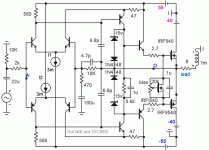
I think I found the sweet spot for the phase compensation capacitors. I was able to use the speed-up emitter resistor/capacitor in the mosfet gate drive circuit with the increased stability. I found the folded cascode feedback approximately doubles the frequency response of the amp. The delay with a 0.1v 10mhz input was 27ns. The distortion at 1mhz read about 3.6%. The crossover artifact was about 15 to 20ns as seen on the 1mhz wave.
Hi jam,
I apologize if this circuit has pushed the limits on capacitor count according to the criteria you had mentioned for this thread.
Hi Charles,
I have not given up on shunt feedback. But I think I temporarily became frustrated with it.
Hello Graham,
I think I found the sweet spot for the phase compensation capacitors. I was able to use the speed-up emitter resistor/capacitor in the mosfet gate drive circuit with the increased stability. I found the folded cascode feedback approximately doubles the frequency response of the amp. The delay with a 0.1v 10mhz input was 27ns. The distortion at 1mhz read about 3.6%. The crossover artifact was about 15 to 20ns as seen on the 1mhz wave.
Attachments
Hi, Subwo1,
Is the compensation you use (6.8p) is the one that Graham pointed?
Folded cascode is faster (than ordinary differential-VAS connection), because emitor drive is faster than base drive?
Is this why the so called modern "current feedback" terminology is faster, because the feedback comes to its emitor?
Is the compensation you use (6.8p) is the one that Graham pointed?
The 2xC+R networks should improve the balance between halves at rf frequencies.
The advantage of applying folded cascode drive from both differential collectors to both VAS emitters is symmetry of operation. A music wave form can have equal chance of a particular excursion in either direction, so it just makes sense to me to enable equal control in both directions. Since cascode drive is faster than base drive, I just figured that it was a way to speed up the feedback loop and give the feedback a forward boost in time. That sounds simplistic, but nonetheless, sums up that aspect of what I was thinking.
Folded cascode is faster (than ordinary differential-VAS connection), because emitor drive is faster than base drive?
Is this why the so called modern "current feedback" terminology is faster, because the feedback comes to its emitor?
Subwo1,
Looking good. Don't forget the gate resistors for the output mosfets. I might be inclined to put the Vgs multiplier before the drivers.
Regards,
Jam
Looking good. Don't forget the gate resistors for the output mosfets. I might be inclined to put the Vgs multiplier before the drivers.
Regards,
Jam
Hi subwo1
I was beginning to lose the absolute phase track myself trying to express the way in which shunt feedback loudspeaker induced errors that can occur.
Your post 161 circuit.
Do you have L in series with load, almost any amp can be fast with series inductance ?
It is possible that your symmetrical 6.8pF components are intentionally a local VAS+Output stage feedback, for stabilisation of the 'normal' input signal path, whilst retaining fast response via the folded NFB side ?
Are both 0.1uF caps necessary ? This might tie the VAS collectors together and prevent an ON-going half from correcting an OFF-going error wrt the summed output.
Crossover artifact. Did you mean that crossover took 15nS, or any NFB induced ripple due to that event took 15nS to settle ?
Is the use of those two 0.1uF caps slowing down the crossover where it might be faster with one ?
Did you have the same degree of crossover delay before you added the Miller connected 6.8pFs. Don't forget that the effect they have upon the input stage is 6.8pF multiplied by the VAS stage gain, which might be 1,000 (or more?) the VAS collector is buffered by emitter followers; ie. Miller C.eff = 6.8nF working against 560R.
Crossover delay might have an insignificant effect upon forward steady state observations, but it can sound bad when a reactive loudspeaker load shifts current crossovers away from the zero voltage line and the NFB loop loses control during that crossover time period. A sudden loudspeaker induced error is generated during the time delay when the NFB loop is not in control, which it then corrects, the result being a zig-zagging effect which is superimposed upon any forward distortion. This low level sharpness from ordinary frequencies can modulate tweeter waveform.
Class-A amps do not do this, and represent a simple solution.
I have found the postings about Mosfet gate capacitance etc. very interesting, this kind of information does not seem to be readily available elsewhere.
Cheers ............. Graham.
Hi lumanauw,
These 6.8pF caps are in a slightly different spot than the 2C+R method. Like Graham was thinking, I placed them near on the VAS bases because that was as close to the folded cascode input as I could get. I had tried to make a version with basically a type of Siklai (sp) pair out of the mosfets and the gate drivers with the 6.8pf caps then going to the VAS emitters, but the circuit was harder to get its currents in balance and it needed floating power supplies on the driver (gate buffer) transistors' emitters.
I definitely think this reason is for it, and also why I am still trying to come up with a new configuration something like that one.🙂 I just think jfets are a little weak in that capability.
These 6.8pF caps are in a slightly different spot than the 2C+R method. Like Graham was thinking, I placed them near on the VAS bases because that was as close to the folded cascode input as I could get. I had tried to make a version with basically a type of Siklai (sp) pair out of the mosfets and the gate drivers with the 6.8pf caps then going to the VAS emitters, but the circuit was harder to get its currents in balance and it needed floating power supplies on the driver (gate buffer) transistors' emitters.
Is this why the so called modern "current feedback" terminology is faster, because the feedback comes to its emitter?
I definitely think this reason is for it, and also why I am still trying to come up with a new configuration something like that one.🙂 I just think jfets are a little weak in that capability.
Hi jam,
Thanks. I noticed the gate resistors are missing and should be included for reliability purposes. I think I will try it with the Vgs multiplier before the gate drivers because then quite a few components can be eliminated. I hate too many parts.🙂
Thanks. I noticed the gate resistors are missing and should be included for reliability purposes. I think I will try it with the Vgs multiplier before the gate drivers because then quite a few components can be eliminated. I hate too many parts.🙂
Hi Graham,
that phase stuff can get to a person.🙂
The L is there because I noticed on some designs, sort of like you mentioned, that the performance can be altered by its presence. Since I use an amp for each separate driver (or series or paralleled), I like to see if the circuit can handle the out of phase current draw--does that idea match what you were thinking?
The 6.8pF caps were originally on the emitters of the VAS to give them the fastest effect, but when I reconfigured the circuit that location no longer had the correct phasing.
I use the 0.1uf is to speed up the mosfet gate turn-off and keep them more in lock-step so as to maintain more constant bias set. I noticed on some mosfet amp designs that cross-conduction can become somewhat a problem at high frequencies. One reason why I want the circuit to be fast is that I plan to use it in a class H subamp and want the fastest possible response to reject tracking rail ripple. I don't think the second one is needed because the drain-source impedance of the Vgs multiplier is low with the heavy on-bias.
The crossover artifact is a 27ns flat spot as seen when driving an 8R with a 1mhz signal. I thought that it is good and in no way audible. I actually see it as better than biasing the mosfets too high since I think doing that may reduce power supply rejection. Since the flat spot at crossover is only on the negative going slope, I think it is due to the slower turn-on of the P-ch mosfet. I think it means that the crossover took 15ns. That is 10x faster than the actual switching frequency of the fastest class D amps.
I temporarily removed the miller caps and the crossover period was still there. I think it shows that the circuit is fast. As per jam's idea, I moved the Vgs multiplier before the mosfet buffers. The performance is about the same with the loss of four parts, two of which I should have included earlier. I realized that a resistor must connect the emitters of the gate buffers together or else the gates will float up! I used a 1k resistor and a 1uf cap.
I do see some of that zigzagging instability you mentioned when the amp comes out of clipping with either a resistor or resistor plus inductor load. I know one way to reduce this problem is to bias the VAS on slightly and I did just that change. I expected that I would see the distortion increase, but the lower open loop gain didn't increase distortion much this way if at all. In the past I lowered the gain by connecting high valued resistors between the VAS collectors and bases and found that I had to lower the gain so much that the distortion increased 10x. But, really, this may actually sound better because it makes the amp softer, more stable, and more predictablek with the loss of constant VAS current with different rail voltages. Now I simply hooked the current sources to the VAS bases instead of the power rails.
I also found the gate discussion interesting. Thanks and best regards.
Attachments
Inverting topology
Hi subwo
I once posted a symmetric inverting circuit here: http://www.diyaudio.com/forums/showthread.php?s=&threadid=7058&highlight=
I have only played with P-SPICE so far. Actually I even roughly calculated a version that is a little more refined than this one. A friend of mine wanted to try it out but didn't have the time to do so, neither did I. I didn't simulate THD up to the MHz range but simulations showed almost the same figures for 1 kHz and 20 kHz.
BTW: The "batteries" are just simple voltage sources. Because I have only the trial version of P-SPICE, I can't use too many "real life" models, so Zeners, pots and the like have been substituted by voltage sources. Neither are the devices used very "sexy".
When I "experimented" with the circuit, I started off with a simple circuit with just two stages (somehow looking like an inverted version of a Hiraga circuit). I soon saw that I wouldn't get the load independancy and bandwidth I was looking for. Also did I have to use much too low values for the input and feedback resistors (at least for my taste). Furthermore did I want a highly biased output stage but not class-A.
Regards
Charles
Attachments
Hi Charles,
Thanks for posting your circuit. You have stated earlier your preference for inverting circuits., but what about the drawbacks for example the feedback network is hooked up to the input and has a relatively low impedence and could be affected by the source ( possible instability) and would a buffer in front of the input help by isolating it.
I have always pondered that that question, I know many manufacturers use inverting circuits (even Mr.Pass) but has anyone done a study of their advantages vs disadvantages.
Reqagrds,
Jam
Hi Charles,
I agree, simulations do not always translate to real circuits flawlessly. I used transistors inferior to the ones I really want to use for the same reason you did. The specs on the circuit as far as distortion look good. I suppose you wanted common source output to simplify power supplies. But it is good with low power supply rails where high output bias is not critical, and good frequency response is still possible.
I agree, simulations do not always translate to real circuits flawlessly. I used transistors inferior to the ones I really want to use for the same reason you did. The specs on the circuit as far as distortion look good. I suppose you wanted common source output to simplify power supplies. But it is good with low power supply rails where high output bias is not critical, and good frequency response is still possible.
Subwo1,
The circuit is looking good. I would suggest that you replace the Vgs multiplier with one like Mr.Pass uses in the A75 ( He always does everything for a reason 😉 ) because if the trim pot fails the unit won't go to full bias and blow the output stage.
We all expect you to build this amplifier when the design is complete.
All,
As, further note, anyone that is inclined to use this topology should read Mr.Pass' atricle on the A75 which is located here
http://passdiy.com/legacy.htm
It is a great primer for this sort of design. To me, and I have stated this before the A75 is one of the most amazing diy designs out there, and has been mostly ignored (because of it's complexity?) designs available to diyer's. It can be scaled back and is still an excellent performer. I have built two of them and would put them up anything out there.
Regards,
Jam
I was wondering if anyone else has built or seen this topology used in commercial equipment. I enjoy the sound of quasi-comp amps, and I’m always looking through patents, web sites, or whatever looking for information on quasi amp’s, and recently I found this patent by two Japanese fellows (patent 3,813,606) describing a unity gain phase shifter that looked interesting.
I modeled it in Pspice and then built it but I can’t see the unity gain of the phase shifter and am wondering if this really works or not. I imagined that the two transistors comprising the phase shift would need to be very closely matched to counteract each other, but I don’t get a unity stage I get a gain on the real model. Any thoughts?
I modeled it in Pspice and then built it but I can’t see the unity gain of the phase shifter and am wondering if this really works or not. I imagined that the two transistors comprising the phase shift would need to be very closely matched to counteract each other, but I don’t get a unity stage I get a gain on the real model. Any thoughts?
Attachments
I like inverting circuits because there are only resistors that are not within the feedback loop. While they are in no way perfect they are still the one component that behaves closest to their theoretical behaviour (of all known components).
I am aware that this topology definitely affects the signal source. That's why I introduced Q15 and Q17. They are something like an "internal buffer" (actually an incorrect description, since they are part of a folded cascode), allowing higher values for R11 and R24 to be used, than without them. Which in turn decreases interaction with the driving source.
I did however not make any close analysis of this interaction but an inverting topology is definitely a case of moving a problem to somebody else.
The topology itself is quite fast with two inner feedback loops and one global feedback loop.
The first feedback loop is around Q16 and Q8 for the "upper half" and Q5 and Q7 for the "lower half" of the circuit, via R37 and R38. The second innner loop is consisting of the Sziklay output stage with gain. I have first seen this type of output stage in the German mag Elrad, but it seems to come from an Australian mag originally (the original circuit that used it has also been posted on this forum at least once). I like it because you can use lower-voltage driver transistors like the BD135 to 140 series which are quite fast (I have used some of them for transmitters !) and it still has some gain that increases overall NFB.
Regards
Charles
Edit: This post is refering to post #169 (I am a little slow when it comes to typing).
I used MPSA92/42 for the differential and current mirror also for the ccs for the differential but not the vas ccs. mje340/350 for the vas and 350's in the unity phaze shifter and 340's for the output transistor pre-drivers. Fairchild's flj4315's were used in the output stage. Amp sounds great but I don't have any expensive equipment to do any real test on it's performance.
Attachments
i felt induced to reply
"I vote for Dieckmanns. This would be expressed in:
Amps per Farad per Volt. I / C / V"
You what makes this truly funny is my middle name is Henry( who would make such a terrible thing up)! That would make it too confusing even for me. Why does this remind me of that useful conversion of the units for velocity into Furlongs per Fortnight?
"I vote for Dieckmanns. This would be expressed in:
Amps per Farad per Volt. I / C / V"
You what makes this truly funny is my middle name is Henry( who would make such a terrible thing up)! That would make it too confusing even for me.
Why does this remind me of that useful conversion of the units for velocity into Furlongs per Fortnight?Okay subwo
All bases covered and it won't need a specialised pre-amp.
I'm clean out of suggestions !
Hi Charles,
I see that you have no input capacitor. Well done.
I once design/simulated a 600 ohm input shunt feedback JLH variant, with the intention of building a matching 600 ohm pre-amp.
But heck no-one else would have the same, so I dropped it. Also with my present universal circuit I would not choose to try that path again.
Easyamp.
That circuit might be good until you run it loudly. With reactive back emf demands the VAS can sink much more current than the CCS; also, although your VAS stage will not have very high multiplier gain, there is a Miller C.dom - hopefully of very tiny value. Your circuit might have a much lower residual distortion if you implement the 2xC+R feedback I mentioned to subwo, also an output Zobel might help.
Is that soot on your proto board ?
I thought I had the monopoly on building solid state arc lamps !
You know they say that you never learn unless you make mistakes, well I've been learning for forty years now - there's always new mistakes to make !
Must catch up with the thread, it has been moving fast.
Cheers ............ Graham.
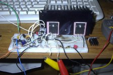
I have unfortunately ended the life of a few devices prematurely but all in the name of education.
I have two of these proto boards and the other is worse, I melted down the leads on 2 ndp7050's after converting my test citation 12 to fets when something happened I'm still trying to figure out, and I forgot fuses. The ends of the leads are now fused to the insides of the proto board, I just tried to photo it but you can't really see the leads sticking out so you'll have to use your imagination. I actually had to cut one of them off the heat sink because the screw had fused to the tab of one the fet's.
The schematic and the picture were a concept I was trying to figure out not a yet fully designed up amp. I've got emf backtalk diodes on the actual amp.
Cheers
Hi Graham,
thanks for your help! You were a tough critic, but I feel the effort paid off.
Hi Charles,
that makes sense about the least nonlinear components being outside the feedback loop. I couldn't quite put my finger on why I had a certain liking for the shunt feedback method.
thanks for your help! You were a tough critic, but I feel the effort paid off.
Hi Charles,
that makes sense about the least nonlinear components being outside the feedback loop. I couldn't quite put my finger on why I had a certain liking for the shunt feedback method.
updade on the circuit above
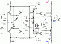
I think I made a lot of progress on the AB circuit since I wrote the text above. I found a better location for the phase compensation caps. The better way is a little different. It places the first cap in the standard location and the second connects from one of the VAS collectors back to the feedback transistors' bases. Now the circuit shows simulation stability driving any capacitive load, I tested it to 10uF, when driving .1uF, the bandwidth is still over 1mhz.
Now, I am giving the slew rate instead because I am not sure that the 2mhz bandwidth can be given as the figure since I am not sure if parasitic resonances are building up over time, for example in the mosfets, which make the bandwidth look higher than actual. So I am giving the figure of 150v/microsecond.
Another change to note is that the lower 1N4148 is backwards.
Thanks, all.
- Status
- Not open for further replies.
- Home
- Amplifiers
- Solid State
- Amplifier Topologies