I think you are not easy to drive The TPH3206, the switch speed is too fast, easy to self-OSC, the PCB layout requirements are also high, you can try TI's drive all-in-one device, better to use , of course, Navitas is also a good choice, we try to use these devices on the 300-500 100V amplifier, At present, it seems that the effect is perfect.
300W-500W 100Vrms output,attach a screenshot of the GaN power output stage。
Attachments
I was considering doing something like this. But all existing half-bridge drivers have problems with the implementation of protection, or are not adapted for working with bipolar voltage. It is especially difficult to make a good multi-loop FB modulator with unipolar power and full bridge output stage.
In itself, the bridge, in addition to the advantage in the absence of a pumping effect, still has a number of serious drawbacks.
- two output chokes
-Two extra transistors
-6dB worse output parameters
-complication control circuit
At the moment, the board on irfb5615 and other standard parts produces 400W RMS.
optimum dead time turned out 3.3ns
And there are no problems with the thermal interface.
Ahead test for IRFB4227.
Last edited:
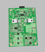
new PCB mono amplifier 3.05 is ready.
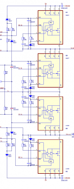
output half-bridge stage on the SI8244 driver
output filter on wima MKP2 polypropylene capacitors
op-amp and modulator power regulators 7812/7912 + TPS7A49 / TPS7a30
On-board preamplifier
preamplifier without capacitors.
servo in the preamplifier circuit
Thermal protection
undervoltage protection
separate overcurrent protection for positive rail and negative rail.
output DC bias protection
STBY
SMPS_OFF signal
Last edited:

Nice built, Bro.
The silicon lab driver is very nice,it's easy to adjust the deadtime, only the over current protection need external circuit.
The silicon lab driver is very nice,it's easy to adjust the deadtime, only the over current protection need external circuit.
Very good. The comparator analog part count for the current monitor and temperature monitor could can been eliminated in favor of an MCU.
Basically all these function(s) can be written in firmware with a few passives interfacing to an ADC.
Thermal protection
undervoltage protection
separate overcurrent protection for positive rail and negative rail.
output DC bias protection
STBY
SMPS_OFF signal
I'm keen to share my MCU implementation with you that does the above with additional features.
Last edited:
Thanks, Erica!Nice built, Bro.
The silicon lab driver is very nice,it's easy to adjust the deadtime, only the over current protection need external circuit.
yes, I had to sweat to create a full-fledged high-speed current protection
Thank, Reactance!
MCU, of course, it is more convenient.
But there is no way to debug yet. In addition, the high level of switching noise of power st. sometimes makes bad jokes with MCU.
MCU, of course, it is more convenient.
But there is no way to debug yet. In addition, the high level of switching noise of power st. sometimes makes bad jokes with MCU.
Thank, Reactance!
MCU, of course, it is more convenient.
But there is no way to debug yet. In addition, the high level of switching noise of power st. sometimes makes bad jokes with MCU.
I'm sure power stage switching wont effect it, too much unproven believes 😀
debugging is easy, the code is written independent, challenge is critical events
are services is the shortest possible time. I can 20uS at the moment with monitoring Voltage, Current, x3 Temp Sensors and I2C as a slave service.
firmware can help with other interesting things like gated overload example: if 10A is overload allow 10A+ for 100ms. This can happen alot with audio at high volume subwoofer applications, watching movies ect..
It is clear that it is in principle possible. But I have no such opportunity. I applied the overcurrent protection with a time delay of less than 500ns. There are pros and cons to this solution, but it's already implemented on the PCB and works great. I'm too lazy to redo a good design
- Home
- Amplifiers
- Class D
- Amplifier module on driver SI2833