Hello,
I newer to this forum .Recently I'm trying to build an Amplifier .For this I have taken a circuit from http://sound.westhost.com/project27b.htm .But the thing is the PNP Transistor (Numbered BD140) which is connected to the MJ3055 is getting heat within few minutes whenever switch on the circuit.I can't find out the problem and proceed forward.So pls help me to complete the amplifier.Here I'm using the Power supply +/_30 volts railing.
Best regards
Madhu
Hi Madhu,
Check the connections to the 2N3055's are correct. Bring the amp up slowly and watch the bias current.
-Chris
Check the connections to the 2N3055's are correct. Bring the amp up slowly and watch the bias current.
-Chris
Honey,
Have connected the BD140 and BD139 on the heatsinks , since these are CFB forming pairs, their temperature compensation must be adequately implemented..... apart from that is your connections are wired right , check the connections and proceed further.....
Have connected the BD140 and BD139 on the heatsinks , since these are CFB forming pairs, their temperature compensation must be adequately implemented..... apart from that is your connections are wired right , check the connections and proceed further.....
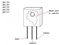
Amplifier Circuit
Cris,
thanks for your sugession.I don't know how to measure the BIAS CURRENT .Rest of this every thing ok on my circuit.So please let me know how to measure the bias current .
Best regards
Madhu.
Cris,
thanks for your sugession.I don't know how to measure the BIAS CURRENT .Rest of this every thing ok on my circuit.So please let me know how to measure the bias current .
Best regards
Madhu.
About measuring the bias current:
there are 1ohm rated power resistors between the collectors of the output devices and the output of the amplifier.
let's measure the DC voltage on these resistors.
you know, I=U/R
so, for example, if the voltage is 100mV-DC, then the current is: Ibias=0,05V/1ohm, so 0,05A=50mV
there are 1ohm rated power resistors between the collectors of the output devices and the output of the amplifier.
let's measure the DC voltage on these resistors.
you know, I=U/R
so, for example, if the voltage is 100mV-DC, then the current is: Ibias=0,05V/1ohm, so 0,05A=50mV
Hi all
I went through that and measured the bias voltage across the resistor(collector to the out put ) is zero.And I observed that in the circuit Veb of the out put -NPN transistor (2N3055)as 10.2 Voltage.But the Vbe of the -PNP transistor(MJ2955) is 0.7 votage.Please let me know what might be the problem.
with regards
Madhu
Hi Madhu,
Measure across the 0R1 resistors in the emitter lead. It sounds like the E-B connections are reversed biased (or open - ouch). The 220R resistor may be open, also the 0R1 resistors.
-Chris
Measure across the 0R1 resistors in the emitter lead. It sounds like the E-B connections are reversed biased (or open - ouch). The 220R resistor may be open, also the 0R1 resistors.
-Chris
Hi anatech,
Ok I measurd the voltage as 0.2 voits.Tha resistor(220 ohms) working well .You said that"may be E_B reverse biased".If it is right what about complimentary transistor.I hope you will clarify my doubt.
Ok I measurd the voltage as 0.2 voits.Tha resistor(220 ohms) working well .You said that"may be E_B reverse biased".If it is right what about complimentary transistor.I hope you will clarify my doubt.
Hi Madhu,
Okay, 0.2V means 2A per device. That is going to run hot.
To check the outputs. Collectors should measure 2R between them (NPN & PNP). The NPN emitter goes to the negative supply, 0R1 resistance, the PNP goes to the positive supply, again 0R1 resistance.
Is that how they are actually installed?
-Chris
Hi anatech
In your last post you said that "use 2ohm resistor instead of 1R at out put stage transistors".Then also no improvement.Ok.my doubt is -with 1R biasing the NPN transitor shows correnct biasing voltages but PNP is out of the biasing.What might be the reason.I hope you clarify my doubt.
Best regards
Madhu.k
Hi Madhu,
I was suggesting you measure the voltage across each 0R1 resistor to calculate the current through each transistor. You will also determine the amount of current sharing.
The forward voltage drop of a power transistor at bias is normally in the range of 0.55 ~ 0.62 VDC. The reverse E-B breakdown can be 6~8 VDC. The only thing I an think of to get approx. 10 VDC is reverse bias or open connection.
The best way to check the junctions is with the unit powered down and supply discharged. Use your ohmmeter to check the emitter base junctions and connections back to the VAS circuit. Work slow and pay attention.
-Chris
Hi Every one!
I found some problems in my previous circuit.So that I am trying another one ,this time the amplifier out put showing some distortion in positive peak.But negative peak is ok.I am hopefully
waiting for your clarification in this regard.
Regards
Madhu
I found some problems in my previous circuit.So that I am trying another one ,this time the amplifier out put showing some distortion in positive peak.But negative peak is ok.I am hopefully
waiting for your clarification in this regard.
Regards
Madhu
Hello Carlos,
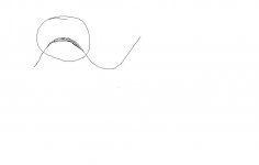
Thanks for your suggestion. Once again I verified every thing on my circuit board.But still I getting the signal on CRO with distortion.Now I am attaching the file of what type of problem I am getting actually.I hopefully waiting for your reply.
Regards
Madhu.K
Thanks for your suggestion. Once again I verified every thing on my circuit board.But still I getting the signal on CRO with distortion.Now I am attaching the file of what type of problem I am getting actually.I hopefully waiting for your reply.
Regards
Madhu.K
Attachments
Hi Madhu,
I think we've all had that problem. I had to increase the standing current to a predriver to solve mine. Do you have a zobel network on the output?
-Chris
I think we've all had that problem. I had to increase the standing current to a predriver to solve mine. Do you have a zobel network on the output?
-Chris
Have you mounted the diodes together on the same heatsink as the Bd139/140 transistors? (hard to do this i know)
I dont really like that circuit. I would prefer higher emitter resistors.. 0.33R or so and get rid of those diodes and add a Vbe multiplier instead 🙂
You also might have oscillations because of the tight local feedback loop in the CFP output. Have you made a PCB of your own or did you buh from Rod Elliot (the site)?
Hello,
Thanks for your suggestions.Mr.Fritzell, for this circuit the designer not recommended heat sink for Bd ic's. And you suggested that 0.33 or higher emitter resistor. I am using 1 ohm resistor at each emitter.How can I replace diodes with Vbe multiplier.I have prepared my own PCB.If you have any circuit details for Vbe multiplier plz let me know.
Mr.Chris, I am not using Zobel net work. At present I am not connecting to any Speaker load.Instead of that using Dummy load(10 ohm resistor with 20watts).
Regards
Madhu.K
Have you made a PCB of your own or did you buh from Rod Elliot
Significant question because it is a CFB circuit. The PCB layout can be a factor. Sometimes it is hard to determine why there is an oscillation and when you finally cure it is can be a puzzle to figure out why the cure worked. This is similar to the P3A and I assume that Rod has worked out the peculiarities on his PCB.
First suggestion: re-melt all the solder joints, a not quite perfect joint can act like "diode like" (per JLH), which is not a desirable trait. BTW this is much more likely to be helpful than the suggestions that follow.
Second suggestion: check your wiring layout to be sure the input signal wires are kept away from the output transistors and wires. This applies to the PCB layout as well if you made it yourself.
Third suggestion: Try increaseing the value of the Miller compensation cap (220pF) in steps. This is an inelegant way to deal with your problem, but sometimes it helps.
Fourth suggestion: Ignore the problem if you can get the fuzziness down to where it's not too prominent. People smarter, more experienced and more iknowlegeable than I have have written that small CFB oscillations are benign and do no harm. Considering who it is that writes this, it must be true 😉 but it aggravates me none the less.
- Status
- Not open for further replies.
- Home
- Amplifiers
- Solid State
- amplifier circuits