My lateral amp have for some reason started latching the bias to 1.5-1.6A on startup, ignoring the bias pot, i have to turn it off, adjust bias to 0 and then it'll start up just fine.
It dident do this before i put it aside to built a dc/overheat protect.
I noticed the VAS is running way hot, could this be causing the problem ?
It dident do this before i put it aside to built a dc/overheat protect.
I noticed the VAS is running way hot, could this be causing the problem ?
No oscillation what so ever, its rock stable right up to clipping and beyond.
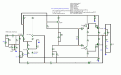
The circuit is like thjis but with dual output pairs: http://i.imgur.com/kiwus.jpg
The rails are 50V and with that it gives 155 watts before it clips into 3.9 ohms.
The circuit is like thjis but with dual output pairs: http://i.imgur.com/kiwus.jpg
The rails are 50V and with that it gives 155 watts before it clips into 3.9 ohms.
Last edited:
I don't understand the operation of the circuit.
What is Q5 doing?
Why are there no source resistors on the 2pair output stage?
Why is the input LTP operating with unbalanced currents and voltages?
Why is R8 there?
How far does the maximum unclipped output voltage drop when changing from 8r0 load to 4r0 load?
What is Q5 doing?
Why are there no source resistors on the 2pair output stage?
Why is the input LTP operating with unbalanced currents and voltages?
Why is R8 there?
How far does the maximum unclipped output voltage drop when changing from 8r0 load to 4r0 load?
I don't have a 8 ohm dummyload so i cannot test that.
I've seen on this forum that with laterals you don't need the source resistors.
Q5 inverts the signal so that two N channel devices can be used.
This circuit is based on the citation 12, in cact the resistor values around the LTP are the same, 680 and 15k. Just slightly different values in the feedback and bootstrap, other than that it is the old citation 12 circuit.
R8 is what i use to null the dc offset.
Hi,
duplicate the drive to the other Nchannel. See how Quasi did his quasi FET amplifiers.
Both FETs need to see the same signal.
I am suspicious of the 1k5 as the load for Q5.
What are the currents in R10 and R17? They should be exactly 2:1 ratio.
You should not need to set output offset by adding such a large value resistor as R8.
Buy a job lot of 5W wirewound resistors so that you can assemble a selection of high dissipation 4r0 and 8r0 dummy loads.
Two 4r0 and one 8r0 allow 1r6, 2r0, 2r67, 4r0, 8r0, 10r0, 12r0, 16r0 dummy loads.
Or just make 4 identical 4r0 dummy loads using 10off 10r0 for each load. That also allows 1r0 and 1r33 loads as well.
is it oscillating?
I support the 'does it oscillate' question.
It has been noted that differential input pairs will sometimes oscillate in the 100MHz-even GHz region (you won't ever see that on your scope) and the result is shifts in DC. It has even been reported (by the famous French writer Héphaïstos) that a differential pair will completely block an output transistor while this even isn't visible on the scope.
Even a small wiring problem can give this effect.
just by twopence.
albert
I don't understand the operation of the circuit.
What is Q5 doing?
Why are there no source resistors on the 2pair output stage?
Why is the input LTP operating with unbalanced currents and voltages?
Why is R8 there?
How far does the maximum unclipped output voltage drop when changing from 8r0 load to 4r0 load?
With advise like this...........
Why do you bother posting........
is it oscillating?
I had the same issue of "bias lockup" on one of my new BX mongrels. One module had a misplaced 100R IPS degeneration resistor (10r instead - way too high UGP/low phase margin). Before I fixed it , I could turn it off , reduce the tail current with "CCS adj." The bias would be right. Music played , scope showed no oscillation until several hours later or if I increased the tail current. My oscillation was at about 2.4 mhz and intermittant ,I replaced the resistor ... all was well. The OPS survived but showed that "hairpulling" latch-up symptom corresponding to what is described. The bad voltage stage did the same thing on 4 other OPS's as well (warm zobel , "latchup"). One stupid 10R degeneration resistor after I changed every device in the whole board... 😱😱
Give the poor amp at least a set of small drivers (mje340/350 or mpsa92/42) , and like Andrew suggested .. use quasi's method for the OPS , degenerate the VAS/IPS some (more). Too simple for a 120W+ amp ... good for a 20-40w student amp.
OS
Last edited:
I think im gonna hook up the board from the godzilla project, that has all the bells and whistles in current mirrors, current sources and all that jazz.
I think im gonna hook up the board from the godzilla project, that has all the bells and whistles in current mirrors, current sources and all that jazz.
You want one that is a good start ? (below) you don't need ALL the "bells and whistles" , but a few essentials are best. (IPS CCS / drivers).
R9 is bias adj. r22 keeps outputs under 1A if r9's wiper screws up (bad pot)
OS
Attachments
Henry,With advise like this...........
Why do you bother posting........
I ask the questions because I do not understand how the amplifier is supposed to work. If the OP can provide answers to these questions and show that the amplifier will work set up this way then he should be able to solve his problem.
But he comes here asking advice.
Now he needs to go back and find which if any of these "errors" in set up might be a cause for his problem, or is it something else?
Seems like it doesent like starting up without a load. I left it on long enough to time out the dc protector delay and as soon as the speaker relay flicks on, the bias drops down to the set 150-200mA.
So it might be dc offset related, this thing sits at 150 some mV offset when working. If i remove R8, dc offset shoots up to like 250mV.
I think a current mirror is needed to minimize dc offset without using R8.
So it might be dc offset related, this thing sits at 150 some mV offset when working. If i remove R8, dc offset shoots up to like 250mV.
I think a current mirror is needed to minimize dc offset without using R8.
Member
Joined 2009
Paid Member
Wow, this thread is a weird coincidence. I experienced this problem at the weekend as I am putting a pair of my amplifiers through more rigorous testing. One of my boards has a bias instability - the output device bias moves up and down with a 30s period. Secondly, if I hook up a long heavy nasty speaker cable instead of a short one, the output is blocked - sound goes in the front, nothing comes out the back. I thought my CD player had gone duff. I remove the speaker cable and use a shorter one, sound comes back. No oscillations visible on the scope, cold zobel. I'll be adding an output inductor for starters and revisiting the LTP.
The driver board have been replaced with this: http://i.imgur.com/bgCAY.jpg
Based on a design by Quasi, this is working perfectly fine, settles right as the set 150mA no matter if theres a load or not and only was 20-30mV dc offset.
The real life values arent identical since i don't remember what i put on this board when i made it a few months ago.
However the 200ohm resistors are 470ohm irl.
Okay this is weird!!😕
On 100-200mA bias i get massive what looks like crossover distortion as the sine comes up from neg to pos and as i turn the bias down to zero, this phenomenon disappears and xover dist go invisible on the scope.
On freqs below 1kHz this is not an issue but from 1k and up it gets worse.
Is it that laterals dont want any bias or is it an incompability issue ?
Okay this is weird!!😕
On 100-200mA bias i get massive what looks like crossover distortion as the sine comes up from neg to pos and as i turn the bias down to zero, this phenomenon disappears and xover dist go invisible on the scope.
On freqs below 1kHz this is not an issue but from 1k and up it gets worse.
Is it that laterals dont want any bias or is it an incompability issue ?
Gatestoppers are too high value 2.4K???? should be 220-330. Capacitance of the laterals is causing HF "phenomena". C5 and 10 should go to the rails , as well (B-C shunt- I use this on my triples, 33pF)
OS
Additionally, following the 'oscillations in 100 Mhz's' idea:
try placing a small ferrite bead over the wires (leg) to the Q2 differential base.
The base emitter junction can easily act as diode, upsetting the DC balance.
I have had strange effects too, such as open loop stability, closed loop runaway. One channel perfect, the other 'weird'. My version was for sub.
albert
- Status
- Not open for further replies.
- Home
- Amplifiers
- Solid State
- amplifier bias latchup ?