Hello,
A good while back some one posted this to work out 300W rms into a 8 ohms load. Obviously there will be some voltage lost etc. due to rail sag, device/CCS headroom etc and so on.
Now a question I have is this is obviously for a resistive load and not a reactive load. I was wondering how to factor in phase margins in to the equations.
I am beleiver in having serious current available for low impedance but even a 2 ohm load calculation does not factor in the phase margin.
Just wondering if anyone has a good link or post regarding working this out. I have heard of a 60 degree phase margin being touted about but i wonder what we should really aim for assuming floorstander speakers as a ballpark figure.
Any help/advice appreciatted
Kevin
To work out the voltage rails required all you need to know is:
P = I x V (1)
and
V = I x R (2)
Combining the two gives:
P = V^2 / R (3a)
or V^2 = P x R (3b)
where P = RMS power, I = RMS current, V = RMS voltage and R = resistance, or impedance in this case.
For 300W RMS @ 8 ohms, and using equation (3b):
V^2 = P x R = 300 x 8 = 2400
Therefore V = sqrt(2400) = 48.99V (RMS)
To get peak voltage we have to multiply this by sqrt(2):
V(Peak) = 48.99 x 1.414... = 69.28V
As you said, there will be losses, so you will want a few volts higher than this to achieve the required 300W @ 8 ohms.
actually the phase margin is most important with capacitive loads, and not so important with inductive loads. the reason is that there are phase delays in EVERY amp, and they are unavoidable, and they effect the stability of an amp. the better the phase margin, the better the amp can drive capacitive loads without oscillating. the phase margin is derived by measuring the output phase across the whole unity gain bandwidth of the amp, and subtracting the highest phase angle from 180 degrees. if the amp phase angle crosses 180 degrees before reaching the unity gain frequency of the amp, the amp is prone to oscillation at that frequency, and is unstable. if your phase margin is less than about 45 degrees, you want to avoid capacitive loads. 60 degrees is really good, and probably would be stable with capacitive loads.
the unity gain frequency of most amps is somewhere around 1-3 MHZ
the unity gain frequency of most amps is somewhere around 1-3 MHZ
you have the language slightly wrong, load phase angle is not "phase margin"
[edit: crossing posts; #2 above relates to "phase margin", below I show a sim that calcs device power when the load current phase angle varies - approximating a complex impedance load]
sim can do this too, LtSpice calcs device pwr (hold down alt after tran analysis, click on device body when thermometer appears)
E = sine Voltage
Z = impedance magnitude
phase = load phase angle (degrees) - stepped from 0 to 90 in 30 deg increments
approx slightly off from using independent Isource as load but close enough for most purposes
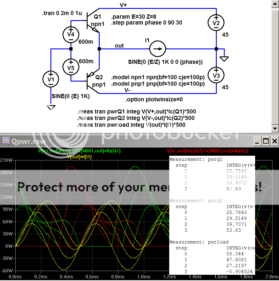
The huge peak device power with 90 degree (pure imaginary) load is clearly visible in the plots
LtSpice file, runs in free Linear Technology Switchercad iii
http://www.linear.com/company/software.jsp
(rename without .txt)
[edit: crossing posts; #2 above relates to "phase margin", below I show a sim that calcs device power when the load current phase angle varies - approximating a complex impedance load]
sim can do this too, LtSpice calcs device pwr (hold down alt after tran analysis, click on device body when thermometer appears)
E = sine Voltage
Z = impedance magnitude
phase = load phase angle (degrees) - stepped from 0 to 90 in 30 deg increments
approx slightly off from using independent Isource as load but close enough for most purposes
The huge peak device power with 90 degree (pure imaginary) load is clearly visible in the plots
LtSpice file, runs in free Linear Technology Switchercad iii
http://www.linear.com/company/software.jsp
(rename without .txt)
Attachments
Hi Fanuc,
Bensen posted a spreadsheet that combined load phase angle with FET output stage and incorporated device SOA to allow modelling of reactive loads vs SOAR.
This is based on an article by David Eather, "A Practical Approach to Amplifier Output Design", Silicon Chip, February 1991, pp.14~18 and April 1991, pp.64~67
I have modified that sheet for FETs and for BJTs and included temperature derating, second breakdown, protection locus (for some BJTs).
Email if you require copies.
Hello,
Thanks for the replies. Yeah you were right JCX, I shouldn't of used the term phase margin - this caused some confusion. Sorry about that. Should be load phase angle!
Thanks for the simulation looks interesting.
A question for you by the way (off topic), regarding Walt Jung's super regulator. I remember you discussing with Walt about using a different type of compensation that permitted large C's on the output. Is it difficult to use that sort of compensation ?
I would love a copy Andrew if you would. Thanks
Kevin.dabson(@)gmail.com - Please remove the brackets
Thanks for the replies. Yeah you were right JCX, I shouldn't of used the term phase margin - this caused some confusion. Sorry about that. Should be load phase angle!
jcx said:you have the language slightly wrong, load phase angle is not "phase margin"
[edit: crossing posts; #2 above relates to "phase margin", below I show a sim that calcs device power when the load current phase angle varies - approximating a complex impedance load]
Thanks for the simulation looks interesting.
A question for you by the way (off topic), regarding Walt Jung's super regulator. I remember you discussing with Walt about using a different type of compensation that permitted large C's on the output. Is it difficult to use that sort of compensation ?
AndrewT said:Hi Fanuc,
Bensen posted a spreadsheet that combined load phase angle with FET output stage and incorporated device SOA to allow modelling of reactive loads vs SOAR.
This is based on an article by David Eather, "A Practical Approach to Amplifier Output Design", Silicon Chip, February 1991, pp.14~18 and April 1991, pp.64~67
I have modified that sheet for FETs and for BJTs and included temperature derating, second breakdown, protection locus (for some BJTs).
Email if you require copies.
I would love a copy Andrew if you would. Thanks
Kevin.dabson(@)gmail.com - Please remove the brackets
Fanuc, yes Walt Jung SR is off topic. I ran some simulations and yep, it does not like it. It scared me off using these other than for localised regulation.
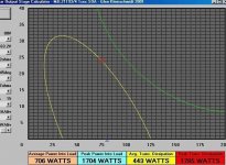
Here is a little program I wrote a while ago for this kind of thing.
It's only very primitive; the green line is the 1sec SOA for the MJL21193/4. The program does not allow for temp-derating, but it will tell you important things such as the average and peak power dissipations of both the transistors and the load for 0-90 degree phase shift.
This information can give you an instant idea of your heatsinking requirements (which is what I mostly wrote the program for).
One day I'll write a fully featured version, with the SOA's for all popular audio output devices included, with temperature derating of the SOA curves, as well as Iq selection to make it usefull for class A designs as well.
The .exe file here:
http://homepages.picknowl.com.au/glenk/calc.exe
For the program to run, this file must be placed in the same folder:
http://homepages.picknowl.com.au/glenk/VBRUN300.DLL
Cheers,
Glen
Attachments
Fanuc said:Hello Glen,
Nifty! I like it!
No worries 🙂
Oh, and in case anyone is wondering, the average transistor and load power dissipation values are not calculated nor approximated with a simple formula.
The program computes the average from the summation of the several thousand instantaneous current and voltage calculations made to plot the graph. In other words, they’re rather accurate.
Cheers,
Glen
One minor little idiosyncrasy of my program that’s worth a mention (before someone picks me out on it 😀 ) In order to calculate a pedantically accurate power dissipation figure for the output transistors, the program takes into account the power dissipated in the emitter ballast resistors. The “Vpeak Load” setting in this regard is a bit misleading. The voltage set by this slider bar is in fact the voltage at the emitter(s) of the output transistor(s). This is why, when you change the “Emitter res.” value, you’ll see the load voltage and current values alter slightly. In order to compensate for the voltage drop across the ballast resistor(s), you just have to bump the “Vpeak Load” value up a little bit.
I never got around to adding the single line of code required to do this compensation automatically!
Cheers,
Glen
I never got around to adding the single line of code required to do this compensation automatically!
Cheers,
Glen
Hi,
average power dissipation of the output devices in reactive loads sounds very useful.
That allows one to insert sensible Tc values into Bensen's sheet to see the long term and transient excursion towards the dre-rated SOARs.
average power dissipation of the output devices in reactive loads sounds very useful.
That allows one to insert sensible Tc values into Bensen's sheet to see the long term and transient excursion towards the dre-rated SOARs.
G.Kleinschmidt said:One minor little idiosyncrasy of my program that’s worth a mention (before someone picks me out on it 😀 ) In order to calculate a pedantically accurate power dissipation figure for the output transistors, the program takes into account the power dissipated in the emitter ballast resistors. The “Vpeak Load” setting in this regard is a bit misleading. The voltage set by this slider bar is in fact the voltage at the emitter(s) of the output transistor(s). This is why, when you change the “Emitter res.” value, you’ll see the load voltage and current values alter slightly. In order to compensate for the voltage drop across the ballast resistor(s), you just have to bump the “Vpeak Load” value up a little bit.
I never got around to adding the single line of code required to do this compensation automatically!
Cheers,
Glen
Hi Glen,
I am working on a spreadsheet to caslculate protection circuit component values related to SOA and (reactive) load lines. Problem is (for me and MS Exel) that it is difficult to have a Vce - Ic based graph and include the reactive load line into it.
There are a whole family of reactive load lines dependent on instanteneous frequency anyway, isn't it.
Douglas Self recommends using a straight line as the "envelope" of all possible reactive lines.
The result wopuld be as follows. Suppose you have 8 ohms resistive, this is a line through Ic=0, Vce=Vsupply (ignoring losses etc) and Vce=0, Ic=Vsupp/Rload; then the envelope of all possible reactive 8 ohms load lines would be a line through Ic=0, Vce=2*Vsupply, and Vce=0, Ic=Vsupp/8ohms.
Can you agree to this logic?
Jan Didden
janneman said:Douglas Self recommends using a straight line as the "envelope" of all possible reactive lines.
Jan Didden
Douglas Self is wrong in this regard.
Hi Janneman,
have you read David Eather, "A Practical Approach to Amplifier Output Design", Silicon Chip, February 1991, pp.14~18 Part 1 and Part 2 of the same article, from Silicon Chip, April 1991, pp.64~67
appendix 4 of http://home.alphalink.com.au/~cambie/ETI466Web.htm#DiffAmp
The number cruching in there was the basis of Bensen's spreadsheet. It shows SOAR and reactive load lines on log/log graphs. Excellent for constant value signals.
I don't know how it could be extended to transient signals. The transient SOAs are easily added on. It's the transient signals and transient protection locus that I cannot get to.
Andrew thanks, I will study the material.
I'm not at transient stuff yet, but have got the steady-state stuff pretty well covered I think. except that reactive load line.
Jan
I'm not at transient stuff yet, but have got the steady-state stuff pretty well covered I think. except that reactive load line.
Jan
mikeks said:
Douglas Self is wrong in this regard.
Mike,
Any pointers to how I should approach it?
See attached.
Jan Didden
Attachments
Hi,
I started with graphs like your PDF posting.
I could not make sense of it when trying to extend to reactive loads.
Bensen pointed me to Eather.
I started with graphs like your PDF posting.
I could not make sense of it when trying to extend to reactive loads.
Bensen pointed me to Eather.
mikeks said:Refer to SOA prot. paper.
Yes, I know exactly where it is. Some 228km from here. It'll have to wait till Friday...
Jan
AndrewT said:Hi,
I started with graphs like your PDF posting.
I could not make sense of it when trying to extend to reactive loads.
Bensen pointed me to Eather.
Andrew, Mike,
Thanks, but I think I posed the wrong question. I know how to calc the reactive loadline, see attached.
The problem is that I cannot for the life of me get that graph on the SOA graph.
This maybe an Exel issue. The SOA graph is organized as pairs Vce, Ic, in increasing Vce.
The reactive thing is in increasing phi and also the steps are unlike the SOA Vce steps. If i include the columns of the reactive table with the SOA tables it looks gobbledigook...
Jan Didden
Attachments
- Status
- Not open for further replies.
- Home
- Amplifiers
- Solid State
- Amp power calculations into different phase angles