Hi, EVA,
I also think there is something wrong that makes the high-side gate resistor is much hotter than the low side gate resistor.
Since there are some suspects, how to know which one is making this?
I'm using a mix of forced clock and UCD feedback. When clock is removed, auto-oscillating about 350khz, while the clock is 375khz.
Hi, Charles,
How to cure parasitic resonances? Is it looks like jitter (blurry, multiple shadow trace)?
How to cure parasitic resonances? Is it looks like jitter (blurry, multiple shadow trace)?
The four most important things to look at are:
1.) Layout
2.) Layout
3.) Layout
4.) Decoupling
Make sure that your layout uses the smallest possible areas within current loops and make sure to have a proper groundplane.
Regards
Charles
1.) Layout
2.) Layout
3.) Layout
4.) Decoupling
Make sure that your layout uses the smallest possible areas within current loops and make sure to have a proper groundplane.
Regards
Charles
hi,
Better alternatives for the older IR2010-2113 are the IR2181, IR2184 from International Rectifier.
ST Microelectronics also provides high quality high low side MOSFET driver - L 6384 to L 6388. These internally contain the bootstrap diode.
Better alternatives for the older IR2010-2113 are the IR2181, IR2184 from International Rectifier.
ST Microelectronics also provides high quality high low side MOSFET driver - L 6384 to L 6388. These internally contain the bootstrap diode.
Hi, Charles,
Comparing groundplane and layout with care of current loop (like fig7 and fig8 of IR's AN-1135). Which is more important? Can I make good PCB only caring the currentloop, without groundplane? The problem with groundplane is that while the tracks have to be as wide as possible (to make low parasitic inductance), putting groundplane below wide tracks equal to make parasitic capacitance.
Comparing groundplane and layout with care of current loop (like fig7 and fig8 of IR's AN-1135). Which is more important? Can I make good PCB only caring the currentloop, without groundplane? The problem with groundplane is that while the tracks have to be as wide as possible (to make low parasitic inductance), putting groundplane below wide tracks equal to make parasitic capacitance.
Hi, EVA,
After reading that appnote, a little question pop up in my mind. Ground plane (-rail plane for a design using high/low driver), besides give parasitic capacitance (can do both positive and negative effect (like parasitic capacitance to inverting input) to a different cct), they also give low inductance+low resistance path for current loop, say for Vgs loop.
Could it be that the positive effect of ground plane is actualy this good loop path itself? For example, many designs make good Vgs drive (track width, track length), but forgetting about the return current (like nF cap from source of the mosfet back to the+ supply of the high/low driver)? This is helped much by groundplane. Ordinary track is inferior to groundplane if we look at this aspect.
Ground plane [...] also give low inductance
Could it be that the positive effect of ground plane is actualy this good loop path itself?
(I'm not Eva, but) Yes, most of the times!
Could it be that the positive effect of ground plane is actualy this good loop path itself?
Yes and it is making your reference "rail" the least inductive that is possible.
Regards
Charles
OK.
I might be wrong here. Anyway, here's an example for this discussion. If we are tracing the Vgs-loop, shouldn't the left side of C9 connected to +9V (instead to gnd), and left side of C8 connected to gnd (instead to +9V) to complete the shortest Vgs loop? And add another 100nF cap from +9V to gnd?
I might be wrong here. Anyway, here's an example for this discussion. If we are tracing the Vgs-loop, shouldn't the left side of C9 connected to +9V (instead to gnd), and left side of C8 connected to gnd (instead to +9V) to complete the shortest Vgs loop? And add another 100nF cap from +9V to gnd?
Attachments
Since the gate driver is referenced to ground (and therefore its output voltage as well) also the output device's source should be referenced to ground.
BTW I have a circuit using such a capacitive coupling for the gate-drive signal but with a high impedance DC path in parallel. This one can do 0 to 100% duty cycle.
Regards
Charles
BTW I have a circuit using such a capacitive coupling for the gate-drive signal but with a high impedance DC path in parallel. This one can do 0 to 100% duty cycle.
Regards
Charles
Hi, Phase_Accurate,
Do you mean C8 and C9 is better the original way than my suggested modification above?
Do you mean C8 and C9 is better the original way than my suggested modification above?
Don't know the original. But C9 is correct in your post. C8 I would reference to ground as well but the driver IC should have some decoupling across its supply as well.
Regards
Charles
Regards
Charles
Hi,
Seeing as it is a level shifting complimentary driver and output stage, it kind of seems like JohnW got the bypassing right, just like it is. He does tend to know what he's doing though.
The Driver P channel is the pos. 9V rail connect to driver source, driving the Vgs of the P chan output, with it's source "referenced" to the High voltage rail. Shortest loop seems to be across the two. It's quite the backwards thing to look at though.
Do also note that the output stage is completely AC coupled to the driver, and as such likely uses bipolar supplies, where its DC references are either rail.
You should link to the thread where you found the circuit so that it can be viewed in its proper context.
Hi Lumanauw,
...I would also guess that there is a fast decoupling cap across the SI1539DL, like Charles is proposing.
You got this schematic from JohnW and did not discuss with him about the layout? He has his own philosophy, which is working pretty good.
...I would also guess that there is a fast decoupling cap across the SI1539DL, like Charles is proposing.
You got this schematic from JohnW and did not discuss with him about the layout? He has his own philosophy, which is working pretty good.
Hi lumanauw,
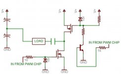
The circuit you have shown using p-channel and n-channel MOSFETs looks rather complex. Since you are using p-channel MOSFET as high side switch, implementing the simple level shifting method, the circuit can be made much simpler than what you have shown.
The two external driver ICs could be eliminated and an NPN transistor-resistor-zener could be used for level shifting the p-channel MOSFET while the n-channel MOSFET can be driven straight from the PWM chip. If you are using chips like SG3525, gate drive current should not be a problem as the SG3525 (with its internal totem-pole stage) can provide enough current to drive the MOSFET at frequencies greater than 100kHz.
What I have just said can be easily understood if you look at the circuit I have attached here.
To everyone,
I have not used PCB but have tested the circuit on verroboard / stripboard. I have used my circuits successfully upto 132kHz with no problem. The only consideration, as what I see, is that the tracks/ traces should be kept as short as possible. Decoupling capacitors should be placed where necessary and should not be omitted.
_____________________________________________________________________________
The strongest man in the world is one, who stands alone for achieving something good.
পৃথিবীতে সেই সবচেয়ে শক্তিশালী ব্যক্তি, যে ভাল কিছু অর্জনের জন্য একাই নিরন্তর চেষ্টা চালিয়ে যায়।
Attachments
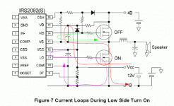
This is what I understand from fig.7 of IR's AN-1135
The lower mosfet turn on is the pink loop. The basic thing is that everytime a current is sourced, it must come back, in this case the +/- of the capacitor.
The loop started as charge stored in the +cap (this cap is the one between pin10 and pin12). This charge goes to pin12, then sourced by pin11, goes to lower mosfet's gate.
After going to the gate, this charge has to come back, from gate it goes to lower mosfet's source, flowing in -B rail, and ends at the -cap (the one connects to pin10). This means that cap has to be a fast one (tantalum or ceramic). Many designs put electrolytic//with 100nf. I think the charge of this loop goes mainly through the 100nf, not the electrolytic cap.
This agrees with loop formula, the current goes in and out should be 0.
Usually the analysis stops at the mosfet's gate, and overlooked what happens next. This fig. helps me to understand the loop. The path from mosfet's source until -cap has the same importance as the path from +cap to mosfet's gate, since they carry the same charge. If the later one is bad, the former will be affected with the same degree.
Attachments
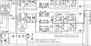
In this schematic, the charge starts as +cap of C319, to pin3(Vcc), to pin1 (LO), to mosfet gate (Q309-311), to mosfet source, to R346, ramping through -rail, then go back to -cap of C319. The problem is that C319 is only 1000pf, E309 is not used. This means, the charge has to travel a longer way to the -rail+12V generator (Q303's capacitor) E315 (on the lower left).
Attachments
Hi, Tahmid,
That cct is not mine, it is property of JohnW, a member here. He's a good designer, but I haven't seen him post on classD forum lately.
That cct is not mine, it is property of JohnW, a member here. He's a good designer, but I haven't seen him post on classD forum lately.
- Status
- Not open for further replies.
- Home
- Amplifiers
- Class D
- Alternative for IR2xxx series