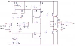
OK. Got the attached circuit on the breadboard. after finding my usual idot attacks it seemed to be working perfectly. Then I got up to 1k and noticed a little distortion. get to 10 or 20k and it's down right hideous. so I am thinking i need to look at the feedback path. Any suggestions from the elders? (in this case elders has nothing to do with age....but knowledge). Thanks guys
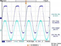
Oh the second attachment is the out put at 10k......Have an FFT of it as well bit i think we can all guess that there is alot of nasty stuff on that one.
Oh the second attachment is the out put at 10k......Have an FFT of it as well bit i think we can all guess that there is alot of nasty stuff on that one.
Attachments
what transistors are you using? and have you tried increasing the current in the input and VAS stage, from that plot it almost looks like your circuit is slew rate limited and then saturateing.
Hi sauuuuuce,
It strikes me that the values of your R6 and R7 are way too high, also that you have insufficient differential input stage current for 20kHz accuracy with a 100pF VAS connected C.dom.
I would not have R4 higher than 100 ohms and R6/7 above 47 ohms.
100 ohms in series with input might also help limit hf overload.
Have you measured the output stage quiescent current ? Expect 10 to 20mV between Q7 and Q9 emitters..
Cheers .......... Graham.
I'm not elder than enybody here (my experience is poor) but:
1.as mentioned before:R6,R7 are too high
2.You Vbe multiplier should regulate base-to-base voltage to set accurate biasing- but I guess it is drawing mistake
3.what is your idle current- have you measured voltage drop on R16/R17???
4. I would throw out C5- the voltage thru emmiter resistor may be as big as 1V. - would it work correct then???
reason for this ugly 'sine' I think is overdriven differential stage
also you may diminish R13
cheers and good luck
Sauuuuuuce,
It's difficult to be definitive without building it and measuring it down to the last root Hertz, so here goes......
1. Degeneration on R6/R7 is huge because your LTP stage current is about 1.24mA, so 0.62mA down each leg. At 600R degeneration, you will have 370mV across each, which, given the VAS will have around 630mV between base and emitter, leaves less than 260mV Vce on the current mirror device. This is not sufficient. Reduce the R6/R7, as Graham remarked, to 100R.
2. A current mirror will ensure that the currents through the emitters are identical. Since the VAS base is supplied from Q10's collector, and since the VAS base bias will be around 70uA, the two collector legs of the LTP are distinctly NOT equal. Better to simply replace the current mirror with a single resistor of 1150R to ensure LTP balance.
3. Q3 base to output resistance is 10K, but Q2 base to ground is only 1K. These resistance paths must be equal for zero offset with matched 1% transistors. Solution: Increase R25 to 10K.
4. Lag compensation is too high for a 1.24mA LTP stage current. Reduce C3 to 47pF.
5. Rather than use a series RC across the feedback resistor, try using 16pF from collector of Q4 to the feedback node (base of Q3). This is phase lead, much loved by JLH, and it will make the amplifier more tolerant of highly capacitive loads.
6. There is far too much emitter degeneration in the LTP. Reduce the 100R you are using down to 10R. This will raise feedback ratio at high audio frequencies and eliminate the distortion you are seeing at 20KHz.
7. You should be using base stoppers of 10R on Q7 and Q9, as these are 30MHz transistors.
8. I'd be reducing the C5 charge suckout from 1uF to 0.22uF.
9. To enable setting the bias at around 60mA, I'd replace R11 with a 2K trimpot.
10. To promote more bias stability with temperature changes, I'd be increasing emitter degeneration on the output devices from 0R22 to 0R47.
Once this is done, you'll have an eminently stable power amplifier which sounds acerbically clean with microtome accuracy. You may actually love the sound, but some will not!!
Cheers,
Hugh
AKSA,
I have a few questions to your comments.
Item 6:
Are you referring to R13?
Item 7:
Do you mean a 10R resistor between the driver and power transistor?
Item 8:
Why? I thought the point was to lower the AC impedance (?).
Jennice
I have a few questions to your comments.
Item 6:
Are you referring to R13?
Item 7:
Do you mean a 10R resistor between the driver and power transistor?
Item 8:
Why? I thought the point was to lower the AC impedance (?).
Jennice
6) R2, R3
7) in series with the base Q7, Q9
8) This cap has to do work at 100 kHz or above. Good HF properties are a must. 0.22 or 0.1 is better than 1 uF in this sence but 1 uF/63V polyester will probably be OK.
7) in series with the base Q7, Q9
8) This cap has to do work at 100 kHz or above. Good HF properties are a must. 0.22 or 0.1 is better than 1 uF in this sence but 1 uF/63V polyester will probably be OK.
Thanks Per-Anders, you answered the questions very well. Jennice wrote:
Item 6 refers to the Long Tail Pair, Q2 and Q3. Their emitter degeneration resistors are R2 and R3. R13 merely sets the constant current flowing through Q5 which supplies the VAS.
Item 7: Yes, that's exactly what I mean here.
Item 8: It's purpose is quite complex. It is a charge suckout cap, whose purpose is to charge up as the voltage across it increases. This happens as one output device hands over to the other; with increasing current, the voltage across this cap starts to increase. C5 quickly and predictably soaks up the charge across its terminals, pulling charge out of the base region of the inactive output device, switching it off without creating a spray of switch-off artefacts. The result is a cleaner handover, or crossover by another name, and this gives less distortion because it removes the HF artefacts which plague Class AB amplifiers. Note that the value of this cap, and the value of the parallel resistor R15, is related more to the geometry and electrical characteristics of the emitters of the drivers and the bases of the output devices. All this is taking place at audio frequencies; in fact it's the time constant of these two components which is important. I'm suggesting a time constant of 0.044mS, which corresponds to a corner frequency of 22.7KHz, actually beyond the audio range and not strictly related to it.
I hope this answers your questions.
Cheers,
Hugh
Item 6:
Are you referring to R13?
Item 7:
Do you mean a 10R resistor between the driver and power transistor?
Item 8:
Why? I thought the point was to lower the AC impedance (?).
Item 6 refers to the Long Tail Pair, Q2 and Q3. Their emitter degeneration resistors are R2 and R3. R13 merely sets the constant current flowing through Q5 which supplies the VAS.
Item 7: Yes, that's exactly what I mean here.
Item 8: It's purpose is quite complex. It is a charge suckout cap, whose purpose is to charge up as the voltage across it increases. This happens as one output device hands over to the other; with increasing current, the voltage across this cap starts to increase. C5 quickly and predictably soaks up the charge across its terminals, pulling charge out of the base region of the inactive output device, switching it off without creating a spray of switch-off artefacts. The result is a cleaner handover, or crossover by another name, and this gives less distortion because it removes the HF artefacts which plague Class AB amplifiers. Note that the value of this cap, and the value of the parallel resistor R15, is related more to the geometry and electrical characteristics of the emitters of the drivers and the bases of the output devices. All this is taking place at audio frequencies; in fact it's the time constant of these two components which is important. I'm suggesting a time constant of 0.044mS, which corresponds to a corner frequency of 22.7KHz, actually beyond the audio range and not strictly related to it.
I hope this answers your questions.
Cheers,
Hugh
Thanks AKSA,
I think I see your point.
However, lowering the resistors in the long tail pair results in higher gain, which may lead to oscillation if the phase runs away at HF. I had to increase the values in one of my amps to solve this problem, despite caps in the voltage gain stage.
Jennice
I think I see your point.
However, lowering the resistors in the long tail pair results in higher gain, which may lead to oscillation if the phase runs away at HF. I had to increase the values in one of my amps to solve this problem, despite caps in the voltage gain stage.
Jennice
I've tried both ceramic up to 100nF, film up to 1uF and 1uF electrolytic capacitors for 'C5' applications in test circuits
All capacitors reduced cross-conduction across the output devices when leaving clipping at 10Khz [no cross-conduction at all with 1uF]. Some linearity improvement at zero-current crossing was also appreciated at the VAS base current waveform
Ceramics and films reduced phase margin and caused ringing when leaving clipping and also at zero current crossing when the amplifier was underbiased. The 1uF film also caused serious driver cross-conduction when recovering from clipping [too low impedance at HF]
The loosy cheap 1uF 100V electrolytic won because it effectively worked as a RC network at high frequencies [I think ESR was about 0.5ohm] , so it had little or no effect on stability and produced very little cross-conduction across the drivers [and none across the output devices]
NOTE : Paralelling 100nF ceramics with the 100uF 63V rail decoupling electrolytics also caused lots of ringing in the power supplies during clipping recovery and even at zero current crossing. Measurements show that placing 100nF ceramics everywhere is usually a bad practice. I prefer ESR resistive impedances at HF because capacitive impedances here allways produce resonant systems

My experience comes from mosfet amps and I didn't have those problems (didn't notice them 😉 ) but your observation Eva, seems to be reasonable.
ASKA
Do you mean 1150R from collector of Q2 to collector of Q3??? This is in reference to ITEM 2
Do you mean 1150R from collector of Q2 to collector of Q3??? This is in reference to ITEM 2
getting better
I decreased all of the the resistances in the Input stage and there was substantial improvement. 20k is still kinda ugly though. Will providing more current to the VAS help with this also?
I decreased all of the the resistances in the Input stage and there was substantial improvement. 20k is still kinda ugly though. Will providing more current to the VAS help with this also?
Hi sauuuuuce,
Hugh's advice re stabilisation capacitors was good.
Your amp currently has substantial VAS C.dom stabilisation and thus I wonder why R20 and C7 are fitted, you could try temporarily removing these.
You could also try 100nF between the base of Q5 and the +37V rail.
Good luck ............ Graham.
Hugh's advice re stabilisation capacitors was good.
Your amp currently has substantial VAS C.dom stabilisation and thus I wonder why R20 and C7 are fitted, you could try temporarily removing these.
You could also try 100nF between the base of Q5 and the +37V rail.
Good luck ............ Graham.
AKSA said:
3. Q3 base to output resistance is 10K, but Q2 base to ground is only 1K. These resistance paths must be equal for zero offset with matched 1% transistors. Solution: Increase R25 to 10K.
Cheers,
Hugh
Hello Hugh and everybody
I know that in the blameless amp input mister Self do match those resistances, but is that only apply to that type of input ?
Thank
Bye
Gaetan
- Status
- Not open for further replies.
- Home
- Amplifiers
- Solid State
- Almost there........Feedback Problem Perhaps??