Hello
Thank you for all of you for the reply.
wahab I plan to use serious separate PS, I'm not after to use large 10 000uF-s on the PC board.
When that large caps start to charge up you all know what happen.
If I get the right transformer I will go with reg front end PS.
Indeed , separating the PSU is a better option as it will keep
the capacitors far from heating sources.
Small thump not a problem while the capacitors charged but I did notice your advise and I'll take care of that, thank you for the advise!
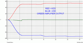
The last update is absolutely necessary as the power on thump
will be reduced to 3V peak over 6 millisecond , otherwise , without
the mod , it will reach as much as 40V for 35 millisecond duration.
I used BG NP caps on the boards, RPR resistors, exotic caps in the PS large Plitron toroid......... close to $$$$ parts value when I count everything including the heatsink, WBT silver solder, connectors etc I do not talk here about the work I invested.
If you go further with this amp just dont throw money in exotic parts,
use whatever you have at hand provided it is of regular industrial quality.😉
Only the transistors should be selected carefully but apart from
the laterals there are quite enough other popular models that would suit
the task for the rest of the circuit.
Can LTspice look at this start up process and can it predict the voltage fluctuations on the output during the first few tens of milliseconds of start up?
Of course , you can either shape the supply voltage output function
or more simply "build" a regular power supply with two generators
and a diodes bridge + filtering caps...
For exemple , using the latter trick , the picture of this thread amp
powering on as it works with the last update discussed a few posts above.
Attachments
Hello
Thank you wahab🙂
Yes first I'll use 1% 1/2W 10Cent metal film resistors. No Dale, PRP etc for test, later I can upgrade.
Capacitors I have some good quality at home, Silmic 100uF, Cerafinen 470uF(RED) or Nichicon MUSE 220uF.
I would have a question, which "transistors" must get some heatsink > I think about the VAS and front end. Power mosfet-s of course!!!
I did check the transistors you picked, it seem some of them are special, not cheap but I'll source them.
If I work on it I want to get a better quality amp than some commercial or GrandMos etc. I know from cheap devices harder to get performance.
I hope we get a decent performance so it will have more interest from other members to!
I work on the layout but need to be total redrawn.. Those in the middle separate are saved for later use..
Thank you very much
Greetings Gabor
Attachments
Yes first I'll use 1% 1/2W 10Cent metal film resistors. No Dale, PRP etc for test, later I can upgrade.
Hi Gabor,
The standing currents are tailored such that the hotter ones will barely dissipate 0.1W , the 0.5W/1% you re using will be more than enough from the start.
I would have a question, which "transistors" must get some heatsink > I think about the VAS and front end.
Power mosfet-s of course!!!
I did check the transistors you picked, it seem some of them are special, not cheap but I'll source them.
As you pointed it, set apart the laterals , the VAS transistors are the ones
that need heatsinks.
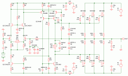
In the schematic below , Q7 has to dissipate 1W while Q8 and Q10 dissipate
0.5W each.
You can mount Q7/Q8 in a common heatspreader if the design need
to be compact , just make sure the heatspreader is efficient enough.
Q11 , the input stage CCS , dissipate 0.16W and need no heatsink in principle.
The other transistors dissipation is negligible and they need no heatsinking.
For Q3/Q4/Q10/Q11 the following models will suit perfectly : 2SC2911/2SC2912/2SC3423/2SC3502/2SC3503/2SC3600/2SC3601
The complementary types are used for Q7/Q8 : 2SA1209/2SA1210/2SA1360/2SA1380/2SA1381/2SA1406/2SA1407
Just take the less expensive ones on the list....😉
Complementarity when chosing among those transistors is not critical , just be careful for the cascodes that must use a pair of the same device.
If I work on it I want to get a better quality amp than some commercial or GrandMos etc.
I know from cheap devices harder to get performance.
I hope we get a decent performance so it will have more interest from other members to!
I work on the layout but need to be total redrawn.. Those in the middle separate are saved for later use..
For performances i think that it s not easy to extract much better numbers from the current design
that reach the essential of two stages amps capabilities , this without compromising stability wich is feature that is not often adressed accurately by most of the designs that hangs on audio forums...
The perfs should be quite good and can be further improved for THD by using a TMC compensation
wich i elected to not implement since it can slightly reduce stability but if you re after the lowest
possible THD i put the mod below so you can choose to implement it or not.
The mod is only around the VAS and it would be easy to go from a compensation to another using the same PCB ,
the components are tailored for minimal TMC effect , to not endanger stability , it allow THD reduction
mainly in the audio band , by 10dB at 1KHZ and about 3dB at 10Khz.
Also , there s no LR network in serial with speaker in the schematic , as such a network position
is to be implemented elsewhere than in the amp PCB.
Eventual values should be 1R in parralel with a 1uH air inductance , about 15 turns of 1mm2 copper wire
around 10mm diameter should do it perfectly.
Attachments
Why do you choose to apply the low frequency roll-off in the NFB (330ms) rather than at the input (4700ms) to the amplifier?
I realise that very little signal will exist at these frequencies, but could such wide-band abilities allow the NFB to interact with the PSU smoothing?
What is the purpose of the forward biased led+diode in the bias voltage string?
Roender implemented a cascode referenced to ground in the other half of the dual VAS. Thus applying ~half rail voltage to all three devices Q7, Q8 & Q10.
Do you see no advantage in such an arrangement, or worse, do you see a negative effect that should be avoided?
Last edited:
Yes , it increase the rejection of PSU VLF as the amp gain is reduced at those frequencies by the virtue of increased global NFB rather than with a passive attenuation at the input
that would left the amp intrinsical gain , thus PSRR , unchanged at those same frequencies.
that would left the amp intrinsical gain , thus PSRR , unchanged at those same frequencies.
Hello
Today finally I finished the layout.
I still have to go over for double check but will look something like these.
Not the easiest layout I ever done it!😱
I do try to avoid to use to many jumper, keep signal away from high Voltage etc. (still I had to use 3 jumper)
There is no power source resistors.
Wahab for R17 & R18 2W resistor will be enough?
Would you please let me know.
Thank you.
Collor codes for the parts
Red transistors-fets
Green Resistors
Grey Jumpers
Blue Capacitors
Purple Diodes,LED
Yellow Trimmers
Greetings Gabor
Attachments
Last edited:
Hi , Gabor
R17/18 dissipate about 0.035W each in normal conditions but at power on they may endure a relatively high voltage/current the time it takes to charge the subsequent capacitors and low TDP film resistors have trouble standing this peak power , so 2W parts are a very good thing in this respect.
As for your PCB , did you use a router ?
Because There s a peculiarity that is odd , Q8 can be simply rotated 180°
then its emitter track to Q6 collector would be shorter as well as its base
track that goes to Q7 base , the positionning of the transistors would be
exactly the same , of course , while the unexpected strap would find itself
totaly irrelevant by the same way....🙂
I saw that you implemented a TMC compensation , should be very
helpfull as it reduce substiancialy THD as well as IMD .
The positionning of the compensation capacitors is great ,
that s optimal in respect of the VAS high frequency stability
wich is to be a concern with cascodes.
@gaborbela, and other users here, I notice that you ignored my remark in a previous post. What you want to do or has done design from Naim, I began to conceive through 2003.
To figure out what is wrong with amplifier diagram posted by you and made from designer to Naim, I recommend viewing below attached project designed by me. DP400 is a project I started when I was in college and during this topic, I thought I outline a final revision. Initials project name is my name.
And please, do not ask me about PCB.
The 2n6800 and 2n6849 are very expensive 23 euro each.
just replace with irf 610 and irf9610 for 1.50 euro each.
Another catch about the PCB....
The current source Q10 on the right extrimity can be turned 90° to the left ,
so the collector track can go in straight line to the trimer and gate resistors
track without having to make half a turn around the emitter hole and with
a much shorter track.
The transistor Q10 would then be aligned between its reference diode and emitter resistor
both wich will stay exactly in the same holes , just the tracks are to be re drawned.
Last edited:
If we look at the latest electronic diagram previously attached, we have already left far target of this topic. They won a regular audio amplifier and what good! You should try to get the "impossible", using only MOS and J-FET transistors. And know that this was possible, just try DP400 project would be a good starting point, it could turn into something much more powerful and better. I could help you achieve this goal impossible, but seeing the direction the discussion took her away, I dropped the idea.
@kees52, I know those 2N transistor are expensive, and yes, you can try 610/9610 although it would be the version to modify a topology diagram and get much more performance.
In fact, I expect it to get to this point, with my help and others. But it was not to be! But it's not wasted time!
@kees52, I know those 2N transistor are expensive, and yes, you can try 610/9610 although it would be the version to modify a topology diagram and get much more performance.
In fact, I expect it to get to this point, with my help and others. But it was not to be! But it's not wasted time!
Hello
Thank you wahab!
I did some mod on the layout, now should be better all do Q5 & Q6 no longer thermally attached to each-other.🙄
Those are cascode only, I think still acceptable these way.
I try to avoid to do anything with Q7 & Q8, a lot of connection around Q8. They are thermally connected.......
I found a bad mistake, I forget to connect Q7 to the base of Q10.
Now that is corrected. One more jumper but what can I do?
I draw all on paint program with out any help. Just think and think...
I'll go over once more to look for errors but I think now these should be OK.
I draw dozens of layout but these was one of the most difficult (took a lot of time and thinking).
Resistors R17 & R18 will goes under the PC board and will be 2W type.
Soon I will post the black layout, if someone else interested on the amp please do not hesitate.
I will help with the layout if you have question!
Thanks one more time🙂
Greetings Gabor
Attachments
Hello
Here is the black layout.
It was (made) designed easily can be used by iron transfer method.
Do not mirror image it. Just print it out with laser printer, iron on the copper clad board, do the eaching and ready for use.
I will do one more check up on the layout but I think is OK how it is.
I moved the input capacitor in to the center of the layout a bit further from the + Voltage.
Any question, advise welcome.
Soon I each the PC board and start test it.. Of course I have to get(purchase) the VAS & other transistors and resistors.
wahab 1W zener diode will be acceptable?
Thanks
Greetings Gabor
Attachments
Last edited:
The hotter zener is the one of the VAS current source , D2 ,
wich dissipate about 0.035W , so 1W give quite a margin...
A few points about the tests process to prevent any bad surprise.
The laterals gate voltage threshold dispersion is quite large on the datasheet
and it can be quite low , the ones on my amplifier are at about 0.25V Vgd
for 100mA current , so usually there s components whose value is to be set
when doing the tests.
As a result when setting your amp use a 100R trimmer instead of 220R ,
and replace the diode that is in serial with the led by a strap, this will
limit the total biaising voltage to 1.2V max value should the trimmer have
a faulty contact , laterals are expensive and one is never cautious enough...
If thoses conditions dont allow to reach a high enough quiescent current
then put a 220R trimmer and remove the strap to put the diode instead ,
all this will extend the biaising voltage range to about 1.9V.
On the PCB i see no boucherot/zobel cell connected to the output ,
that is 10R in serial with 22nF , R31/C5.
Otherwise it can be valuably deported in a separate PCB along
with the output LR network , this will ensure that no significant
AC current run in the amp PCB ground.
that is 10R in serial with 22nF , R31/C5.
Otherwise it can be valuably deported in a separate PCB along
with the output LR network , this will ensure that no significant
AC current run in the amp PCB ground.
Hello wahab
Yes you right!
I know what happened, I left out the source resistors 0R22 and with those I forget the Zobel.
I will put on the speaker terminal if that good enough.
I read some opinion even better than on the PC board.
If you disagree I will try to find some room on the PC board.
To be honest I work on a amplifier Pass F5 turbo V1 enclosure, so I didn't went over on the layout again..
I will do that before I each the PC board! That must be done again.....
Thanks for the warning!
I know you wrote about the bias set up. A bit confusing to me..... To set up the bias it work the same way like at other amplifiers- higher resistance I measure on the trimmer between Collector Q8 & Q10 that cause lower bias?
From your instruction I understood exact the opposite.
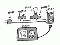
I will use a 100W light bulb something like the att. picture until I set up the bias. If there is any problem the light bulb glows (will take away the current, and that help to minimise the damage)
AndrewT always advise the light bulb at start up...
Greetings Gabor
Yes you right!
I know what happened, I left out the source resistors 0R22 and with those I forget the Zobel.
I will put on the speaker terminal if that good enough.
I read some opinion even better than on the PC board.
If you disagree I will try to find some room on the PC board.
To be honest I work on a amplifier Pass F5 turbo V1 enclosure, so I didn't went over on the layout again..
I will do that before I each the PC board! That must be done again.....
Thanks for the warning!
I know you wrote about the bias set up. A bit confusing to me..... To set up the bias it work the same way like at other amplifiers- higher resistance I measure on the trimmer between Collector Q8 & Q10 that cause lower bias?
From your instruction I understood exact the opposite.
I will use a 100W light bulb something like the att. picture until I set up the bias. If there is any problem the light bulb glows (will take away the current, and that help to minimise the damage)
AndrewT always advise the light bulb at start up...
Greetings Gabor
Attachments
Last edited:
I will put on the speaker terminal if that good enough.
That s the best solution from all points of views.
I know you wrote about the bias set up. A bit confusing to me..... To set up the bias it work the same way like at other amplifiers- higher resistance I measure on the trimmer between Collector Q8 & Q10 that cause lower bias?
From your instruction I understood exact the opposite.
That s it , the lower the resistance of the trimmer the lower the quiescent current , so it should be set at minimum resistance before powering on .
I will use a 100W light bulb something like the att. picture until I set up the bias. If there is any problem the light bulb glows (will take away the current, and that help to minimise the damage)
AndrewT always advise the light bulb at start up...
Indeed mandatory when doing the first real world steps....😉
You can also use the output stage supply rails to supply the front end
for the tests , in fact it will make no difference other than about 20%
less max ouput power , still it will remain roughly over 100W/RMS/8R.
Hello
I can ad the Zobel net. here.
The R18 anyway will goes under the PC board.
What do you think?
Greetings Gabor
In fact , the PCB ground should be separated in two different grounds
that will have their own ground wire that goes to PSU.
The first ground area should enclose all paths that have variable currents,
that is the return ground of the power stage decoupling capacitors
and the one of the zobel network.
The second ground area will enclose all the other grounds return paths ,
that are the ones of the frond end circuitry , including its own decoupling
caps.
Doing this way will reduce vastly eventual ground pollution
induced distorsion and noises.
The layout . . .
Hello Gabor,
Instead of a question, Here rather a nice suggestion. If you'll have any need just PM me and I'd gladly explain the details, You'd be very happy with.
Cheers
Hello
Here is the black layout.
I will do one more check up on the layout but I think is OK how it is.
I moved the input capacitor in to the center of the layout a
Any question, advise welcome.
Hello Gabor,
Instead of a question, Here rather a nice suggestion. If you'll have any need just PM me and I'd gladly explain the details, You'd be very happy with.
Cheers
In fact , the PCB ground should be separated in two different grounds
that will have their own ground wire that goes to PSU.
The first ground area should enclose all paths that have variable currents,
that is the return ground of the power stage decoupling capacitors
and the one of the zobel network.
The second ground area will enclose all the other grounds return paths ,
that are the ones of the frond end circuitry , including its own decoupling
caps.
Doing this way will reduce vastly eventual ground pollution
induced distorsion and noises.
Hello
I agree with you wahab!
I just try to test the amp now to get some idea of the performance.
Later I'll use separate grounds.
Even on simple amplifier (with one PS) I use two ground. I do separate the signal ground from the PS ground with a 10R resistor.
I test the amp and after I'll start to upgrade. Even like these I can get some idea about the sound quality.
At the test I'll use only one PS how you advised. If I like what I'll hear I will increase the front end with 10V rail voltage.
I'll separate the ground even the signal ground.
I just each one PC board for test! After it will be easy to mode the PC board.
Right now I try to keep my PC board a certain size.
Your advise well appreciated! If I like the amp I want min. DALE or PRP resistors, and I'll upgrade the PC board to.
These only a test board, I don't want to mess with PP connection.
Greetings Gabor
- Home
- Amplifiers
- Solid State
- All Hitachi Lateral FET amplifier for DIY described by Paul Kemble