To follow up on my last post, the channel where I thought I saw smoke seems to have stabilized, but the numbers worry me. It has been plugged in for a while with no DBT and is getting nicely warm (nothing concerning) and I'm able to get the offset to stabilize around 0. But here are the readings across the .47 ohm resistors on the outputs and CCS stage that worry me:
R18: .288V
R19: .372V
R16: .497V
R17: 166mV
Thoughts?
R18: .288V
R19: .372V
R16: .497V
R17: 166mV
Thoughts?
I'll have to echo Eric on that a lot of the solder joins look questionable:
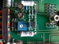
Make sure every connection for every component looks like the smooth transition from pad to wire like on Q7 (green square) on at least one side of the board.
Also either I use way too much solder myself but I'm a little suspicious that when I look at the other components only rarely has the solder has gone through the pad holes to the other side. Makes me think that there might be cold solder joins there too.
Those solder joints look bad on the mosfets because as I said when I posted that pic, I was in the process of removing them with a solder sucker, so please ignore those solder joints. The current joints are clean and smooth. And I've triple checked for cold solder joints. Found one earlier on a small capacitor that I fixed and I'm almost certain that wasn't the problem.
To follow up on my last post, the channel where I thought I saw smoke seems to have stabilized, but the numbers worry me. It has been plugged in for a while with no DBT and is getting nicely warm (nothing concerning) and I'm able to get the offset to stabilize around 0. But here are the readings across the .47 ohm resistors on the outputs and CCS stage that worry me:
R18: .288V
R19: .372V
R16: .497V
R17: 166mV
Thoughts?
Did you match you output mosfets?
Did you match you output mosfets?
I used 4 from the same mouser batch with the same Vgs - 3.22
Even if they are slightly off, would it cause such a dramatic difference in voltages?
There is big difference in the current being drawn for each mosfet. Not being well matched is just one thing it could be. Q5 and Q6 are the output mosfets and should have about the same bias.
How did you measure the Vgs for the mosfets?
I have a Peak Atlas DCA55 semiconductor analyzer.
There is big difference in the current being drawn for each mosfet. Not being well matched is just one thing it could be. Q5 and Q6 are the output mosfets and should have about the same bias.
Exactly. I’m trying to figure out what else it could be.
You bypassed the dim bulb tester before biasing, right?
Never mind. I see it in post #21 now.
Never mind. I see it in post #21 now.
Last edited:
Sorry - but i may demonstrate my self to be out of my depth- but happy to look a fool and learn something...
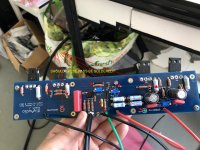
I look at the photo of the pcb and i see tracks going to components and not soldered to them at the pads.
Would it be good practice to solder BOTH side of the board where any componet goes through it?
see attached photo
I look at the photo of the pcb and i see tracks going to components and not soldered to them at the pads.
Would it be good practice to solder BOTH side of the board where any componet goes through it?
see attached photo
Attachments
Why isn't R18 connected in the schematic?
You mean why isn't there a connection between R18 and R13?
The circuitry around Q3 is an overcurrent protection and is sensing the current through one of the output FETs. Look at any Aleph circuit on the net, it's always connected to just one of the source resistors, otherwise the whole current sharing would be messed up.
Regarding the solder joints, if the iron is got enough and with good solder, the pad on the other side will be wetted automatically. Using a higher temp setting can help with this. If you have to resolder a joint, always remove the old solder first. A dodgy solder joint can cause all kinds of trouble in a circuit.
I'm my experience, Fets from the same batch can come well matched indeed. Whether the component tester is performing tests at currents that accurately represent operating conditions is questionable.
Exactly. I’m trying to figure out what else it could be.
It is hard to say without more detective work. Perhaps you need to replace the mosfets and see if that makes a difference. That may be more easy than doing detective work.
It is hard to say without more detective work. Perhaps you need to replace the mosfets and see if that makes a difference. That may be more easy than doing detective work.
As you can imagine, I’m hesitant to buy 8x matched mosfets unless I really have a good reason to believe that is the problem. I’m skeptical. I’ll post some more readings on each leg of the mosfets this morning. Maybe that will provide a clue.
As you can imagine, I’m hesitant to buy 8x matched mosfets unless I really have a good reason to believe that is the problem. I’m skeptical. I’ll post some more readings on each leg of the mosfets this morning. Maybe that will provide a clue.
I can understand but the cost of parts for what you will have when built is really low. I buy tubes of 25 IRFP240 and I have found them to be closely matched. It is entirely possible you damaged the mosfets when the resistors smoked. Since the output mosfets are tied together and also the CCS ones there is only R16 and R17 in their circuit that is the different. Same with R18 and R19 in the CCS circuit. Does the amplifier play as it is now? I doubt there is anything in front of the mosfets that would be wrong if this is the case. At least pull the mosfets and test them again and see what you come up with. You might need to test them on a heatsink and see how the react when they heat up. Every thing you have told us points to the mosfets.
Last edited:
Did you find out more where the pull of smoke might have come from?
If you're making more measurements, please also measure the gate to source voltages
for each mosfet.
Also did you get a full tube from Mouser when you said they're from the same batch?
Your tester quotes a test current of 2.5mA and accuracy of +/-(2%+20mV).
The current is pretty low. Still might not be a deal breaker though.
Did you find out more where the pull of smoke might have come from?
If you're making more measurements, please also measure the gate to source voltages
for each mosfet.
Also did you get a full tube from Mouser when you said they're from the same batch?
Your tester quotes a test current of 2.5mA and accuracy of +/-(2%+20mV).
The current is pretty low. Still might not be a deal breaker though.
I have not confirmed where the little bit of smoke that I think I saw came from, but it appeared near the section of the board with the output mosfets.
Here are the voltage measurements
Outputs
Q7 - G=-17.6V D=-10mv S=-21.5V G to S = 4.13V
Q8 - G=-17.5V D=-8mv S=-22.1V G to S = 4.03V
CCS
Q5 - G=4.06V D=22.6V S=.52V G to S = 3.55V
Q6 - G=3.97V D=22.6V S=110mv G to S = 3.85V
Another thing I observed this morning is that the R27 pot (which I preset at 68K doesn't seem to make too much of a difference to the bias when I turn it. I haven't turned it much because I want to hear back from others on these measurements first, but I'm wondering if that could be a relevant fact.
I bought 16 of these mosfets and they came in the same tube and measured virtually identically. I'm not saying it can't be mismatched mosfets, it's just that I'm not sure it explains the difference in voltage drop I am seeing on the source resistors.
Something looks fishy with Q6/R10.
Can you measure the voltage drops across R9, R10, R11, R12? You probably want to use the mV scale.
Can you measure the voltage drops across R9, R10, R11, R12? You probably want to use the mV scale.
Something looks fishy with Q6/R10.
Can you measure the voltage drops across R9, R10, R11, R12? You probably want to use the mV scale.
They all basically measure 0 or .1mv
I just finished rebuilding the second channel. I installed it and it is also stable now, with higher bias, but stil labout a .3V difference between the source resistors for the outputs. It also has the same close to 0 reading on R9, R10, R11, R12.
One thing I noticed on both channels, and I don't know if it means anything, I can set the bias to near zero, but when the amp is powered off, the bias then rises to about 1.4V before slowly dropping. Is that rise in DC offset upon power off normal for this amp? Could it be a clue as to what is going on here?
- Home
- Amplifiers
- Pass Labs
- Aleph J - Smoke on R17 and R19 - Two blown outputs