The other board is stuffed and is identical. No magic smoke has appeared yet, I'll give it a try.
It might take me a day or two as I haven't drilled the backing plate for the second amp yet. Please bear with me.
The one difference that I see is no link between - input and ground unless I've missed a picture.
One thing that I've noticed is that the working channel is running considerably cooler than the faulty one. I've got the working one making music and it is running a cool 40C on the heatsink. I couldn't detect any oscillation on the faulty channel.
The 100Hz ripple is inaudible under test. I haven't tried applying a speaker to the faulty channel.
The 100Hz ripple is inaudible under test. I haven't tried applying a speaker to the faulty channel.
Last edited:
The one difference that I see is no link between - input and ground unless I've missed a picture.
Hi Marra, you've missed a photo. I've only swapped boards this morning.

Anyone who is following this whole project.
I inherited a beautiful clone of a Pass Aleph 4 which failed, I'm not sure why but it eventually turned out to be a defective bridge rectifier, you can see the amplifier in the top of the photo.
I eventually separated the PSU to prevent further heat failures, you can see the PSU in the bottom of the photo.
It works beautifully but I always felt that it was being restricted by its single ended input, it is a balanced input by design.
I started by building an Aleph P1.7 which is a balanced pre-amplifier but I had no balanced sources.
In the centre of the photo I've got the P1.7 on the bottom with a Kevin Gilmore RCA to XLR convertor and input selector above it. They are both subjects of different threads.
I only built the Aleph J out of curiosity. The one channel that I have got working is certainly very impressive.
Once I get that working 100% the intention is to convert the Aleph 4 to XLR.
The KG / P1.7 / Aleph J are deathly quiet during black passages of music.
Attachments

Last edited:
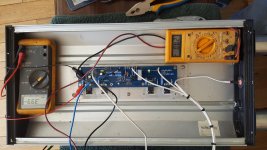
OK - so this is where I am at.
Both modules are fitted into the chassis and wired to their power supplies.
The original faulty channel is still not behaving as it should be.
I have managed to adjust the DC offset to about 150mV and now it is floating between +0.52V and -0.10V which is a lot better than it was.
The adjustment is INCREDIBLY sensitive, the working channel is nowhere near as sensitive.
Bias is fine at 400mV over R16.
One possible clue to the problem ?
On the faulty board Q2 is running very warm. On the working board it is almost cool.
On the faulty board Q2 is running very warm. On the working board it is almost cool.
Ok, I guess I lied. I am still here.
Do me two favours, please.
(1) Stop typing every single sentence into a single post. Try to keep the pieces of information in one post. It makes life so much easier for those who want to help with your issue.
(2) Do what I suggested in post 90 and report back.
Do me two favours, please.
(1) Stop typing every single sentence into a single post. Try to keep the pieces of information in one post. It makes life so much easier for those who want to help with your issue.
(2) Do what I suggested in post 90 and report back.
The voltage at the collector of Q3 is rock steady at +4.81V wrt -24V rail. It is not following the floating output voltage ?
OK
-in, +in and GND are shorted together.
C1 has a link across it.
VGS Q7 = -4.31V, VGS Q8 = -4.37V, VGS Q5 = -4.51V, VGS Q6 = -4.51V all with the negative lead on the gate.
V across R8 = 8.61V
-in, +in and GND are shorted together.
C1 has a link across it.
VGS Q7 = -4.31V, VGS Q8 = -4.37V, VGS Q5 = -4.51V, VGS Q6 = -4.51V all with the negative lead on the gate.
V across R8 = 8.61V
-in, +in and GND are shorted together.
C1 has a link across it.
And R4 is disconnected, right?
VGS Q7 = -4.31V, VGS Q8 = -4.37V, VGS Q5 = -4.51V, VGS Q6 = -4.51V all with the negative lead on the gate.
Looks like Q5 and Q6 (=Aleph current source) turn on harder than Q7 and Q8 (=gain devices).
V across R8 = 8.61V
You previously wrote that R8//R8' = 960Ω. This means the current through R8//R8' is I0 = 8.61V/960Ω = 9 mA. This is about right.
The voltage at the collector of Q3 is rock steady at +4.81V
You previously wrote that R7//R7' = 550Ω. This means the current through R7//R7' is I1A = 4.81V/550Ω = 8.7 mA. This is the current going through Q1A.
The current going through Q1B is I1B = I0-I1A = 0.3 mA. This is way too low. Q1A and Q1B should get about the same currents (about 4.5 mA in your case).
Looks like there is something wrong in the input stage at/around Q1B.
Next steps:
(1) Check for bad solder spots. Start looking at Q1B, and take it from there.
(2) Check the voltage readings: are Vgs at power MOSFETs and voltages across R7//R7' and R8//R8' stable over time? (How) do they correlate with the DC output voltage?
Sorry but R4 was back in circuit.
I've just removed it and the results are the same.
I'll see what happens with a new pair of 2SJ74s.
I've just removed it and the results are the same.
I'll see what happens with a new pair of 2SJ74s.
- Home
- Amplifiers
- Pass Labs
- Aleph J Setting DC Offset