
If I correctly understand your question, the capacitor should be placed to have the shortest physical path distance between the op-amp's output and it's inverting input pins. Placing it across the feedback resistor would lead back through the DAC chip before arriving at the inverting input, which is a longer path. So, I presume they show it placed that way in the diagram (unless there is some other reason) to provide the shortest path length based, and parasitic inductance based, phase-shift of the feedback network at high-frequencies. The capacitor not only performs reconstruction filtering of the signal, it helps to stabilize the op-amp from oscillating under the high-slew rate conditions presented by the signal coming out of the DAC.
Last edited:
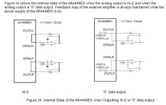
I haven’t reviewed the data sheet of the AK4499. That said, it looks to me that the shorted internal path must be switchable by the DAC. When the path is in the shorted mode, the I/V op-amp simply acts as a unity-gain voltage-follower. Outputting whatever voltage is on it’s non-inverting input. Adding a shorted path outside of the DAC as you drew, would make it non-switchable by the DAC.
What they say is that the internal path keeps the opamp feedback loop closed when the dac is powered up, even if the dac is not playing. What they don't say is exactly why they routed the feedback path through the dac chip in the first place. My guess would be maybe its to compensate for bondwire resistance. Something more or less like that.
I agree with Mark, it looks like a force-sense connection (partial Kelvin contact).
At least at low frequencies, the feedback around the op-amp makes the input impedance at the point where the connection branches into a wire to the feedback resistor and a wire to the negative op-amp input nearly zero. Any resistance of the wire from this branching point to the negative op-amp input has practically no impact, because there is practically no current flowing through it. Any resistance of the wire to the feedback resistor just increases the feedback resistance a bit.
By putting the branching point on chip, they can put the point with near-zero resistance precisely where they need the lowest resistance.