Hi all,
I have made this topic for my upcoming project, AK4458 multichannel DAC. There are not too much multichannel DACs on the market, but I need it to drive my active loudspeaker system correctly.
This chip is reasonably priced and has a simple layout (only 48pin) but still have good enough parameters to build an outstanding DAC I think....
I you have any advice, experience, please share it! Thanks...!
/ alternative could be the ES9016 but ESS does NOT support public designs and the costs of a chip incl. taxes and shipping is horrible! /
I use miniSharc with miniDAC-8 based on AK4440. Having compared it to DIY ES9018 or AK4495 I am sure that AK4440 is a well sounding chip and you cannot go wrong with the better AK4485. Good luck on the project and I hope to have the opportunity to replace miniDAC with your board ;-)
The first question: should I supply the AVDD and Vref pins from the same regulator like the datasheet recommends? Does it make sense the use of shunt regulator(s)?
"Power lines of AVDD and VREFH1-4 should be distributed separately from LDO and etc. while keeping low impedance. If it is not possible, it is recommended to connect a LPF composed by a 10Ω resistor and a 220uF capacitor between VREFL1-4 and VREFH1-4. ... The VREFH1/2/3/4 pin is normally connected to AVDD, and the VREFL1/2/3/4 pin is normally connected to AVSS."
"Power lines of AVDD and VREFH1-4 should be distributed separately from LDO and etc. while keeping low impedance. If it is not possible, it is recommended to connect a LPF composed by a 10Ω resistor and a 220uF capacitor between VREFL1-4 and VREFH1-4. ... The VREFH1/2/3/4 pin is normally connected to AVDD, and the VREFL1/2/3/4 pin is normally connected to AVSS."
Attachments
Last edited:
My secound question: does it make sense to build in a quality oscillator near the IC for the master clock (like by the ESS DACs). Does it improve anything or I should use rather the SCK (or MCK) coming from the receiver?
Based on my experience with Wolfson DACs I'd suggest if you're looking for the best subjective sound quality, arrange for the loading of the audio output pins to be as light as possible. To do this increase the working impedance of the suggested output circuit in fig75. Scaling all the resistor values up by a constant factor and the capacitor values down by the same factor will achieve this. I'd also suggest reducing the corner frequency of this circuit as 99kHz is rather high for a -3dB point.
For the supply rails, you'll want the lowest impedance to get the best performance. Most standard 3pin regulators don't give particularly low output impedance at lowish currents (of the order a few tens of mA). Shunts tend to do much better - transistor assisted shunts better still. Check the TL431 datasheet for a suggested circuit for a transistor assisted shunt.
For the supply rails, you'll want the lowest impedance to get the best performance. Most standard 3pin regulators don't give particularly low output impedance at lowish currents (of the order a few tens of mA). Shunts tend to do much better - transistor assisted shunts better still. Check the TL431 datasheet for a suggested circuit for a transistor assisted shunt.
Last edited:
Thanks. I'll try my own shunts first...🙂
Output filter is another theme, I'll use full balanced output, possibly with OPA1632 IC-s (but it is just an idea).
Output filter is another theme, I'll use full balanced output, possibly with OPA1632 IC-s (but it is just an idea).
Attachments
Last edited:
On the question about Vref, definitely I'd use a separate dedicated regulator for that, preferably with a passive (LC) filter on its output to get the lowest possible noise.
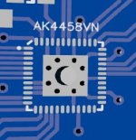
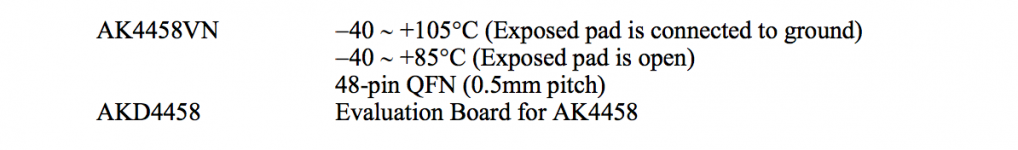
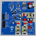
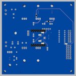
You have seen that this DAC is in a QFN package and you have tools and/or skills to solder this leadless package?
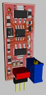
Just a preconcept....
The problems are the really big Vref caps:
- I can't leave the shunt panels in lying position (if I want to keep the 100x100mm panel size).
- If I use the shunts, I think they will be too big for them to work stable. But I need to make some tests before...
The problems are the really big Vref caps:
- I can't leave the shunt panels in lying position (if I want to keep the 100x100mm panel size).
- If I use the shunts, I think they will be too big for them to work stable. But I need to make some tests before...
Attachments

Yes I have seen... I'l try simple with a pointed soldering iron and soldering paste. Bad idea?
I would use solderpaste and a oven.
Soldering iron, not sure? Depends on the QFN variant AKM uses, it might or might not expose the leads on the side (but very small if it is exposed).
I'll buy maybe a mini-soldering iron with 0,1mm tip, like: http://www.ersa-shop.com/ersa-l%C3%B6tkolben-minor-p-2859.html But an oven may be good to...
I'll buy maybe a mini-soldering iron with 0,1mm tip, like: http://www.ersa-shop.com/ersa-l%C3%B6tkolben-minor-p-2859.html But an oven may be good to...
The chip has an exposed pad on the backside which is connected to ground for thermal relief. To solder that you really need an oven or a hot air tool.
You could just put some thermal paste between the pcb and the pad and solder the sides by hand. Looking at the picture of the DAC on the green PCB earlier looks as if the pins go up the sides. I think you could just use lots of flux and drag a ball of solder around to fix it down like a BGA chip. Probably depends on how much practice you have had at doing it or how many chips you are willing to sacrifice to get it right.
The chip has pins going up the sides!
An idea is to place a 1,5-2mm hole in the middle and heating the thermal paste from the bottom to fix the exposed pad on the backside...
An idea is to place a 1,5-2mm hole in the middle and heating the thermal paste from the bottom to fix the exposed pad on the backside...
Attachments
Last edited:
The chip has pins going up the sides!
An idea is to place a 1,5-2mm hole in the middle and heating the thermal paste from the bottom to fix the exposed pad on the backside...
Yep that is another option that will work. If you used solder paste under the chip it would still be able to be removed easily but if you used regular solder through the hole it might be harder.
I was meaning to just use regular heat transfer paste like for mounting parts to heatsinks. As the DAC chip has no pins it won't actually stand up above the board height so a thin layer would aid the thermal relief without having to actually be soldered down.
So where I am not sure that the bottom pad of the chip is only by reason of thermal connection OR must be definitive grounded? The first case would be the easiest (could leave this big hole in the middle)...
Question: what do you think, should I use the built-in 1,8V LDO or rather an external one?
(or make it switchable...)
(or make it switchable...)
Last edited:
So where I am not sure that the bottom pad of the chip is only by reason of thermal connection OR must be definitive grounded? The first case would be the easiest (could leave this big hole in the middle)...
The datasheet lists two temperature ranges for connected or not connected which is why I thought the pad was for thermal relief only.
Attachments
- Home
- Source & Line
- Digital Line Level
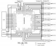
- AK4458 multichannel DAC with I2S input