jacques antoine,
we have to protect ourselves from harmful knowledge. Simulations provide nondepressive knowledge.
we have to protect ourselves from harmful knowledge. Simulations provide nondepressive knowledge.
But your comment about "single diffused transistors" is moot. Transistors built with that technology are obsolete.
Like the 2SK135, which is pretty pedestrian these days. And an on-state resistance of about 1 ohm is not spectacular. A saturation resistance of the TIP3055 is 0.25 ohms.
john_ellis,
the purpose of the hometaxial base technology was to prevent second breakdown by reducing the pressure difference between the emitter and the collector. According to RCA, hometaxial base denotes a single diffused transistor with a base region of homogeneous resistivity silicon in the axial emitter-to-collector direction. Homogeneity refers to structural regularity like that of the pure, weakly conductive silicon dioxide.
Nowadays severely inhomogeneous, toxic, highly reactive (high-k) materials have largely replaced the contaminated silicon dioxide dielectric.
The width of depletion region is small for all modern transistors. What is much more relevant here is that it implies heavy doping since the depletion layer width (volume) is inversely related to the doping level (density) and positively correlates with the built-in potential.
.
A thick depletion layer in conjunction with a homogeneous dielectric greatly enhances signal transfer quality, but that was hardly RCA`s goal. There has been a blatant scarcity of targeted attempts to practically utilize that bothersome combination.
Contrary to popular belief, a low intrinsic resistance, a high input impedance, a high amplification factor, high mobility, a short transit, rise and settling time do not promote signal transfer quality. "Saturation resistance" is a senseless term. "Velocity saturation" makes sense.
N101N,
Where to begin?
I suppose I must thank you for a more lucid explanation. But you still seem to mix things up.
Let's start with the 2N3055. The original hometaxial base transistor started with a p-type moderately lightly doped wafer, and the emitter and collector were diffused into it from both sides of the wafer. That led to the very deep junctions which allowed the depletion regions to be very wide. You talk about "senseless terms" but still use the word "pressure" for voltage. What the wide depletion regions did was to reduce the electric field i.e. voltage over distance, crudely put, so that both ionisation was low and in particular, electrical heating was more widely dispersed in the wider depleiton regions so that hotspot formation was minimised, leading to the better second breakdown immunity.
That technology basically became obsolete when wafer diameters increased from the about 3 inches as the thickness of the wafers also increased to maintain rigidity in processing. The thicker wafers meant you could not longer economically diffuse the junctions in from both sides.
Homogeneity used in the term hometaxial referred to the regular doping level (uniform) in silicon, as opposed to a diffused profile which has some sort of exponential variation with distance. Not referring to silicon dioxide, which is usually described as amorphous. I suppose you could call it homogenous. But a silicon dioxide layer, weakly conducting or not, was not part of the actual transistor unless you think of a passivating layer.
The high-k dielectric you mentioned are mostly used in small geometry, MOS integrated circuits. Integrated circuits of technologies down to 0.35 micron (now old hat) used pure silicon dioxide. "Contaminated" is hardly a true statement of that technology. MOS technology only became feasible when contamination was eliminated from the oxides as contamination caused threshold voltage drift.
Again you mix terms. Small transistors in integrated circuits which have dimensions as small as a tenth of a micron gates or smaller, have to have depletion regions appropriately scaled. That does mean highly doped layers. But the voltages are limited to 3.3V or 1.8V because the electric fields are so high. Small bipolar transistors have forward voltages approaching 1V due to the high doping levels, which would be limited by the silicon bandgap in the end.
Power transistors replaced the old deep diffusion of the hometaxial base transistor with an epitaxially grown collector. You cannot replace the collector depletion region by a narrower one and maintain the breakdown voltage. The emitter junction has always been highly doped in order to reduce hole injection from the base (in an NPN) and the base is now epitaxially grown on the collector layer, so can also be thin and optimsed in doping. These still have base voltages around 0.6-0.7V which tells you that the base doping is still not so high as you suggest for small transistors.
"A thick depletion layer in conjunction with a homogeneous dielectric greatly enhances signal transfer quality".
A dielectric is an insulator. If you mean the base, then it is clearly not a dielectric. It is silicon, however, lightly doped, but still conducts.
"Contrary to popular belief, a low intrinsic resistance, a high input impedance, a high amplification factor, high mobility, a short transit, rise and settling time do not promote signal transfer quality."
I assume you mean a MOSFET by this description. However, once again you make statements without explanation. I'd agree that low intrinsic resistance is not, per se, an indication of signal quality. But "high input impedance" is not necessarily true even in a MOSFET. The gate capacitance means a fair amount of charge is needed to shift the voltage at higher frequencies.
(And I still maintain that voltage is the key controlling element. All of the electric fields and effects in a device are voltage dependent. Charge is needed as a result of trying to shift voltages).
A short transit time leads to a fast response and that implies a better starting point for signal quality. The corollary of a low amplification factor, low mobility, a long transit time do promote signal transfer quality is equally meaningless. It depends on what bandwidth you need. Germanium transistors seem to be a good fit to that description, but could, in the main, barely manage 10kHz in audio amplifiers. Low frequencies might have good quality, though.
"Saturation resistance" is a senseless term. "Velocity saturation" makes sense.
Saturation resistance is a robustly defined term as the minimum collector(drain) to emitter(source) voltage for a given base current(gate voltage). It is relevant only in terms of an amplifier as to the output voltage which can be provided before clipping occurs. There will be an increase in distortion, however, before that point especially if (bipolar) transistors have quasi-saturation effects which reduce the gain at low voltages. Though the good old RCA 2N3055(H) did not exhibit quasi-saturation so maintained a low distortion to the point of clipping.
Velocity saturation, the maximum velocity electrons or holes reach, is a different phenomenon to saturation resistance.
Correction - saturation resistance is of course minimum CE (DS) voltage for a minimum collector (drain) current, not base(gate). The base(gate) bias of course needed to achieve that applies.
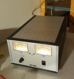
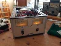
Modified Equin successfully build
After more than 35 years of listening with pleasure to a slightly modified Equin amplifier (the 45V version, with the triples configuration of the original Quad 303 because of stability problems) I decided to build an upgrade from parts I still had lying around, including old TIP35C output transistors. That was a bit too simple.
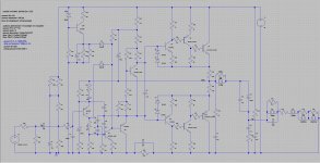
It had to be the 60V version now. For the 45V version I used a stabilized power supply with the then still available L146. My choice for this project was the Elektor Plus power supply from the year 1973.which should be suitable for 60V, but unfortunately that resulted in several transistors going up in smoke. After the discovery of LTSpice I got some insight why and finally I had things working, even with thyristor fall back short circuit protection.
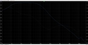
The first attempts to make an Equin amplifier at 60V were disappointing. With the TIP35C as power devices the amplifier oscillated already at a few Watts of output power. (only when the lower transistor was conducting). A fully complementary version with newer TIP35C/36C brought no change. Finally, faster output transistors were the solution: NJW21193&94. With an optimized OLG (LTSpice) everything works stable now, at least on a couple of old bookshelf 2-way speakers (8 ohm). Here, the simulations show an improbably low THD. (<0.001% at 1kHz at ~40W)
I am not an expert in electronics, but have read Self's book and picked up a few things here and there from other authors and in this forum.
After more than 35 years of listening with pleasure to a slightly modified Equin amplifier (the 45V version, with the triples configuration of the original Quad 303 because of stability problems) I decided to build an upgrade from parts I still had lying around, including old TIP35C output transistors. That was a bit too simple.
It had to be the 60V version now. For the 45V version I used a stabilized power supply with the then still available L146. My choice for this project was the Elektor Plus power supply from the year 1973.which should be suitable for 60V, but unfortunately that resulted in several transistors going up in smoke. After the discovery of LTSpice I got some insight why and finally I had things working, even with thyristor fall back short circuit protection.
The first attempts to make an Equin amplifier at 60V were disappointing. With the TIP35C as power devices the amplifier oscillated already at a few Watts of output power. (only when the lower transistor was conducting). A fully complementary version with newer TIP35C/36C brought no change. Finally, faster output transistors were the solution: NJW21193&94. With an optimized OLG (LTSpice) everything works stable now, at least on a couple of old bookshelf 2-way speakers (8 ohm). Here, the simulations show an improbably low THD. (<0.001% at 1kHz at ~40W)
I am not an expert in electronics, but have read Self's book and picked up a few things here and there from other authors and in this forum.
Attachments
I built this amplifier 40 years ago with the original Elektor PCB and parts and when I switched it on the output transistors blew up due to oscillations. This amplifier is as unstable as a quantum bit. I threw it all in the trash and never looked at it again and after 40 years I never will.

- Home
- Amplifiers
- Solid State
- After 40 years : ready to build EQUIN