"XCX9572L... and a WM8804" is two chips. You might want to read the documentation for XC9572L. From looking at this: Solved: Getting Started with XC9572XL Development Kit - Community Forums ...it would suggest the part is programmed in the same Languages as FPGAs: VHDL or Verilog.
Unfortunately they have removed the answer on how to get ISE working on windows 10. But I guess...
Xilinx ISE 14.7 install for Windows 10 — MicroNova
Further, there are references to a datasheet in order to make sure that the chip is supported in the latest version 14.7, but I could not find those document anywhere.
Last edited:
You can always download and install an earlier version of ISE. Also, you can submit questions to Xilinx support for clarification of what version of ISE you would need.
In addition, you can always make a Windows machine dual boot, Linux and Windows. Although that may be easiest to do with Ubuntu, it may not be the best Linux choice for ISE. Just sayin'
In addition, you can always make a Windows machine dual boot, Linux and Windows. Although that may be easiest to do with Ubuntu, it may not be the best Linux choice for ISE. Just sayin'
Last edited:
ISE is no more. There is a wrap-up version that supports all the current old stuff called ISE 14.7 VM For Windows 10. It runs on Oracle linux in Virtualbox. The last none VM version of 14.7 is not officially supported on Windows 10.
Last edited:
The ISE 14.7 windows 10 version indeed supports the XCs now, no problem there. The Xilinx chip has no PLL, but the WM can multiply the clock rate.
I think the following parallel configuration could work.
XC ---> WM (setup configuration)
Clock -> WM multiply clock (x2) -> XC
Clock -> XC
WordClock -> XC
DataL -> XC -> Read on clock 1
DataR -> XC -> Read on clock 1
XC -> Out on halved clock 2 -> WM -> SPIDF
Which gives an 24 bit output, quite fine. The transmitter also allows for right/left justified I2S mode, so including spaces on the stream is allowed.
So very nice, but few considerations before I order.
- Where may I find some physical SPIDF ports?
- I may want to add USB, is there a ready made solution for either I2S or SPIDF format input. Surely it must be possible given all the dongles that do the same thing but w/ cables.
- Would a PIC microcontroller be sufficient for the task, since I already have a board? Is there a reason why FPGA/CLPD is to be preferred to an MC in a task like this?
Ok, thanks again all. This is going quite nicely, can't wait to make an order.
rfbrw said:You lost me at PLL and WM. I'd comment but I have no idea what is going on.
Sorry, WM is the Cirrus logic transmitter chip you recommended. I couldn't recall the extension so it got left out.
PLL = phase lock loop for multiplying the clock frequency. Although maybe it can still multiply the frequency of the clock. But if not possible, the transmitter can do it.
I think the approach idea is to generate a new master clock and or a new bit bit clock for the time domain multiplexed digital audio so it could then be clocked out as SPDIF, if needed.
Last edited:
rfbrw said:Still don't understand your approach but I'm sure a PIC, a dsPIC for sure, can do it.
Thank you, I will try on one of those first.
The approach is to get the clock speed to 1.5x the original (the original being ~44.1x64 by JP8080 manual). Then the 32 bits per stereo sample in the original speed converts to 48 bits per sample in the new speed, which is 24 bits per stereo sample, a nice number. Without the conversion only 16 bits are possible to extract, which is not good. So, take the clock to the Cirrus logic transmitter, multiply the speed and route to the processor chip.
Then on the processor chip write a buffer to stream the left and right channel samples to their correct positions (streamed now by the original clock), and of course create the world clock stream accordingly.
Finally take the word clock and new data stream to the transmitter for SPIDF export, triggered by the new clock at higher speed.
Oh yea and also export the configuration from the processor chip to the Cirrus logic. I hope it is possible to program this way, there is some test board for it that costs $300.
Last edited:
I have unfortunately been ill and busy so the DIY has been on hold.
On the CLPD, there seems to be no problem converting the format (I have added two extra cycles of delay wrt. the 1.5x clock as everything does not likely line up quite that well in reality).

The I2S output are the top rows on top and the inputs are on the bottom.
Still trying to tackle how to make this work on an MCU. The problem is that the base clock oscillates at ~4 Mhz (44100 x 64). Writing a naive algorithm is about 20 C instructions in the main loop and a lot more assembly instructions. Even optimizing perfectly it would probably take something like 1 Ghz processor to catch every clock cycle. The <100 Mhz PICs certainly have no hope. A bit absurd...
Is the MCU approach viable at all or should I admit defeat? Perhaps there is something I am missing...
On the CLPD, there seems to be no problem converting the format (I have added two extra cycles of delay wrt. the 1.5x clock as everything does not likely line up quite that well in reality).
The I2S output are the top rows on top and the inputs are on the bottom.
Still trying to tackle how to make this work on an MCU. The problem is that the base clock oscillates at ~4 Mhz (44100 x 64). Writing a naive algorithm is about 20 C instructions in the main loop and a lot more assembly instructions. Even optimizing perfectly it would probably take something like 1 Ghz processor to catch every clock cycle. The <100 Mhz PICs certainly have no hope. A bit absurd...
Is the MCU approach viable at all or should I admit defeat? Perhaps there is something I am missing...
#include <xc.h>
#include "head.h"
int Buffer1 [32] = {0};
int Buffer2 [32] = {0};
int sw1 = 0;
int sw2 = 0;
int sw3 = 0;
int sw4 = 0;
int sw5 = 0;
int sw6 = 0;
int sw7 = 0;
int sw8 = 0;
int sw9 = 0;
int wOut = 0;
int k = 0;
int z = 0;
int h = 0;
int n = 0;
void main(void) {
TRISA=0; //RA0 = Word Clock, RA1 = Slow Clock, RA2 = Fast clock, RA3= DataL, RA4 = DataR
TRISC=0b11111111; //RC0 = Data Out, RC1 = wClock Out.
while(sw1==0) //Find the start of the data stream
{
if (sw2==1 && PORTAbits.RA0==0)
{
sw1=1;
}
sw2 = PORTAbits.RA0;
}
while(sw5) // Wait for 14 cycles for the signal to start.
{
if(PORTAbits.RA1==0 && sw4==0)
{
n+=1;
}
sw4 = PORTAbits.RA1;
if (n==14)
{
sw5=1;
break;
}
}
while(1) //Main loop
{
if(PORTAbits.RA1==0 && sw6==1) //Stream the bits into the buffers
{
Buffer1[k]=PORTAbits.RA3;
Buffer2[k]=PORTAbits.RA4;
k=k+1;
if (k==32)
k=0;
}
if (sw8==0) //Wait for 9 cycles
{
if(PORTAbits.RA2==0 && sw7==1) //delay
{
z=z+1;
if (z==11)
sw8=1;
}
}
else //Output the bits from buffers
{
if(PORTAbits.RA2==0 && sw7==1)
{
if (wOut==0)
PORTCbits.RC0=Buffer1[h];
else
PORTCbits.RC0=Buffer2[h];
PORTCbits.RC1=wOut;
h+=1;
if(h==24)
{
wOut=1-wOut;
h=0;
}
}
}
sw6=PORTAbits.RA1;
sw7=PORTAbits.RA2;
}
}
Last edited:
You might have a pretty good chance with a suitable STM32 MCU. There is a lot of info on that general topic out there on the net. One arbitrary example: How to Get I2S working on an STM32 MCU | by David Ramsay | Medium
Otherwise, CPLD probably makes a lot of sense. That is, if you can program one. Not like programming a CPU, so there would likely be some reading and study to do.
Otherwise, CPLD probably makes a lot of sense. That is, if you can program one. Not like programming a CPU, so there would likely be some reading and study to do.
You might have a pretty good chance with a suitable STM32 MCU. There is a lot of info on that general topic out there on the net. One arbitrary example: How to Get I2S working on an STM32 MCU | by David Ramsay | Medium
Otherwise, CPLD probably makes a lot of sense. That is, if you can program one. Not like programming a CPU, so there would likely be some reading and study to do.
That graph is direct from an ISE simulation for the XC chip, the programming was not difficult at all. Still would not like to order all that stuff for single use.
Thanks I will check the article out. Perhaps there is a way to stream a block of bits which makes the operations a lot quicker...
Perhaps there is something I am missing...
A method of reading two datastreams with a 2.8 Mhz bit rate simultaneously ? Still, could be worse. You could be trying to do it with an Arduino.
It is the parallel input that trips up the PIC. I2S and the like would be no problem.
You could try reading the port as a whole. You can then move the two bits from the input data register.
You could try reading the port as a whole. You can then move the two bits from the input data register.
Yes, but the smaller PICs do not have interfaces to read inputs in chunks (SPI inputs), at least not enough inputs to get it all the inputs.
I decided to order a Lattice FPGA development board, and convert direct to SPIDF. The plan is to put the small development board inside the unit. Perhaps an overkill, but it seems the easiest route, and the boards are less than 20€, too. The simulation result...
An externally hosted image should be here but it was not working when we last tested it.
Still one question. How to convert the output to 0.4-0.6 V peak to peak as required by SPIDF, is it fine to have it between 0-1.2V instead (and not -0.6 - 0.6)?
Last edited:
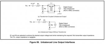
You might consider some interfacing method similar to that shown below.
Attachments
Last edited:
Yes, but the smaller PICs do not have interfaces to read inputs in chunks (SPI inputs), at least not enough inputs to get it all the inputs.
Not that it matters now but you would not be reading via SPI. You would be reading port wide and ignoring all but the two pins required.
Not that it matters now but you would not be reading via SPI. You would be reading port wide and ignoring all but the two pins required.
From what I understood the PIC reads only one bit at a time, when not using any of the interface options. Other than that there are I2S, UART, I2C, SPI and SSC interfaces depending on the unit, to allow reading and writing of multiple bits at a time. But perhaps I understood something wrong? Not that it matters...
- Home
- Source & Line
- Digital Source
- Add a digital out to Roland JP-8000 synthesizer.