Hi I have a ton of tosiba TO3 transistors, and I want to mimick the output stage/power suply of the GFA-555. I want to drive the outputs with a low voltage tube section directely from the line inputs. If you guys could point me in the right direction I would greately apreciate it.
Thanks
Ben
Thanks
Ben
Ben,
I think you'll have to use triple Darlington topology in the "finals". Check with the guys over on the "sand" board.
200 W. into an 8 Ohm load requires a 40 VRMS signal. That means your small signal circuitry has to swing over 113 V. peak to peak. You will need about 250 V. on the plate of the vacuum triode driver. A low voltage type, like the 6GM8, will not do, sorry.
The LOW RP - HIGH gm ECC99 is (IMO) a candidate for the voltage amplifier. ECC99 data sheet here.
Thanks for your answer. The standard topology is the Darlington topology. I have to choices here. Either high volatge trasnsformer, or a tube pre. I would still like to hear ideas on use high voltage tubes to drive the outputs. Anyone know of any good reads on this topic. Tube to sand is not very popular in the DIY world. I am looking at doing a tube pre based on the QUAD 405 amp as an experament.
http://cgi.ebay.com/2-X-AUDIO-POWER...5098578QQihZ002QQcategoryZ39783QQcmdZViewItem
http://quad405.com/brochure.html
I have the perfect match transformer, heatsink, and trasnsistors for this project.
Thanks
Ben
http://cgi.ebay.com/2-X-AUDIO-POWER...5098578QQihZ002QQcategoryZ39783QQcmdZViewItem
http://quad405.com/brochure.html
I have the perfect match transformer, heatsink, and trasnsistors for this project.
Thanks
Ben
Ben,
Let's look at the gain structure this project needs. If you constant current source (CCS) load an ECC99 section, a voltage gain near 20 is a reasonable expectation feeding a triple Darlington emitter follower O/P stage. The driver should stay linear as it pushes the "finals" into clipping. So, the driver has to generate roughly 60 VRMS. Don't forget the NFB loop's requirements. 60/20 = 3. The full O/P of a "standard" CDP is 2 VRMS. Therefore, a line stage with some gain is in order.
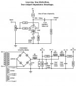
I'm attaching a schematic for a 12B4 based line stage, which WILL get the job done. Look the diagram over and feedback on your observations. Pay particular attention to the pseudo choke I/P filter B+ PSU. The exact value of the "fudge factor" cap. has to be determined experimentally.
Some of the "denizens" of this board developed PCBs for use in constructing CCSes. Those or the Bottlehead C4S will do quite nicely in both the line stage and power amplifier.
Oh yeah, look at the ECC99 data sheet I previously linked. 260 V. on the plate, -10 V. on the grid, and IB = 10 mA. appears to be a suitable operating point. A B+ rail of "300" V. should be adequate to provide for the plate to cathode differential, the 10 V. of bias, and the compliance the CCS load requires. "Full wave" voltage doubling a Triad N-68X will neatly take care of the B+ PSU requirement. You follow the doubler stack with a LC section. CCS loading provides superior PSRR. 🙂
Let's look at the gain structure this project needs. If you constant current source (CCS) load an ECC99 section, a voltage gain near 20 is a reasonable expectation feeding a triple Darlington emitter follower O/P stage. The driver should stay linear as it pushes the "finals" into clipping. So, the driver has to generate roughly 60 VRMS. Don't forget the NFB loop's requirements. 60/20 = 3. The full O/P of a "standard" CDP is 2 VRMS. Therefore, a line stage with some gain is in order.
I'm attaching a schematic for a 12B4 based line stage, which WILL get the job done. Look the diagram over and feedback on your observations. Pay particular attention to the pseudo choke I/P filter B+ PSU. The exact value of the "fudge factor" cap. has to be determined experimentally.
Some of the "denizens" of this board developed PCBs for use in constructing CCSes. Those or the Bottlehead C4S will do quite nicely in both the line stage and power amplifier.
Oh yeah, look at the ECC99 data sheet I previously linked. 260 V. on the plate, -10 V. on the grid, and IB = 10 mA. appears to be a suitable operating point. A B+ rail of "300" V. should be adequate to provide for the plate to cathode differential, the 10 V. of bias, and the compliance the CCS load requires. "Full wave" voltage doubling a Triad N-68X will neatly take care of the B+ PSU requirement. You follow the doubler stack with a LC section. CCS loading provides superior PSRR. 🙂
Attachments
Sweet. I love the simplicity. The power rails on the Adcom GFA-585 are 85vdc(4 separate rails), and have a driver mounted to the output boards. One of my concerns is that the Pre I will be using is 1v out. Is this sufficient? What kind of currant would this tube driver be capable of?
Thanks much.
Ben
PS the GFA-585 requires 2volts for ful output at rated power!!!
Thanks much.
Ben
PS the GFA-585 requires 2volts for ful output at rated power!!!
One of my concerns is that the Pre I will be using is 1v out.
Ben, are you talking about a phono stage or a line stage? The 12B4 based line stage I provided has some gain. So, it will raise the signal from a phono stage or CDP enough to obtain full power O/P.
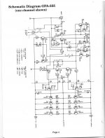
I've attached the GFA-555 schematic. It seems you want to retain the portion to the right of the dashed line. Am I reading your intent correctly? Is control of the idle current present in the 4X matched complementary pairs of O/P transistors retained?
Obviously, the tubed driver works very differently than the SS circuitry. The plate of the ECC99 section is coupled by a pair of caps. to the SS current amplification circuitry. One cap. connects to the "N" side and the 2nd connects to the "P" side.
A DC offset at the speaker O/P can't be tolerated. The "hot" speaker connection also feeds loop NFB back to the ECC99 section's grid. A single common cathode voltage gain block inverts absolute signal polarity. The emitter follower circuitry is non-inverting. That's why the NFB goes to the grid.
Attachments
Eli Duttman said:
1
Ben, are you talking about a phono stage or a line stage? The 12B4 based line stage I provided has some gain. So, it will raise the signal from a phono stage or CDP enough to obtain full power O/P.
2
I've attached the GFA-555 schematic. It seems you want to retain the portion to the right of the dashed line. Am I reading your intent correctly? Is control of the idle current present in the 4X matched complementary pairs of O/P transistors retained?
3
Obviously, the tubed driver works very differently than the SS circuitry. The plate of the ECC99 section is coupled by a pair of caps. to the SS current amplification circuitry. One cap. connects to the "N" side and the 2nd connects to the "P" side.
4
A DC offset at the speaker O/P can't be tolerated. The "hot" speaker connection also feeds loop NFB back to the ECC99 section's grid. A single common cathode voltage gain block inverts absolute signal polarity. The emitter follower circuitry is non-inverting. That's why the NFB goes to the grid.
1 Line level
2 yes, but I was thinking of maybe 6x pairs per channel
3 I do not understand the N,P outputs from the tube. Is it 2 pins?, of 2 polarized caps?
4 I understand.
5 your awsome!, and thanks.
Ben
Ben
Ben,
Please clarify what has a 1 V. O/P level. Obviously, that's not enough to get full power O/P.
"N" and "P" refer to the NPN and PNP sides of the O/P stage. Remember, the driver is a common cathode triode that's CCS loaded. BJTs have to be forward biased. That means each side needs a DC block at the I/P. So, the ECC99 anode is connected to 2 coupling caps., as complementary BJT bias polarities are necessary.
Why 6 matched complementary pairs driving the load? Are you planning on a low impedance load, which draws LOTS of current? If you are going to use 6 MCPs, triple Darlington is (IMO) strongly indicated. The triode drives the 1st BJT, the 1st BJT drives a 2nd, larger, BJT, and the 2nd BJT drives the 6X MCPs. Think of the summed junction capacitance that has to be "manhandled".
I am a little frustrated, and happy😕 today... so I am going to keep it short. I am driving these at 2.6 ohms. I reached 116db today clean with a pot as a pre.
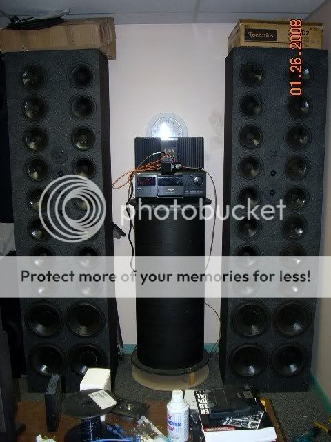
I am driving these at 2.6 ohms.
OK, 6 MCPs driving that difficult load makes sense. Make certain the bipolar PSU you construct has LARGE reserves of current. IMO, triple Darlington is the only way to go, with that many devices in parallel. A 7th MCP, with a fair amount of "heft", is needed in the middle of the cascade. Using the same BJTs as are used for the 6X O/P devices could be convenient.
I'd still like to know what has a 1 VRMS O/P level. 😕
My Outlaw 990 Pre has 1v RMS output, and peaks at 9v. I have no idea why they rate it so low. When I drive my amp directly from the CD player (Sony Changer) I can reach higher clean DB than with my Pre. I made a Passive Pre with a 100k pot, and added a safety DPDT switch to add another 100k in-line to keep the speakers under 100db. So straight to the amp from the CD my distortion lights never flickered, but when driven by the pre they did at 5db lower volume.
Methinks the Outlaw 990 needs to be replaced by a 12B4 based linestage, like the 1 I posted previously.
The circuit I posted earlier will drive the FUGLY IHF "standard" 10 KOhm load and it provides the gain needed in front of an ECC99 driver for a triple Darlington BJT O/P stage. 😉
The circuit I posted earlier will drive the FUGLY IHF "standard" 10 KOhm load and it provides the gain needed in front of an ECC99 driver for a triple Darlington BJT O/P stage. 😉
Eli Duttman said:
OK, 6 MCPs driving that difficult load makes sense. Make certain the bipolar PSU you construct has LARGE reserves of current. IMO, triple Darlington is the only way to go, with that many devices in parallel. A 7th MCP, with a fair amount of "heft", is needed in the middle of the cascade. Using the same BJTs as are used for the 6X O/P devices could be convenient.
I'd still like to know what has a 1 VRMS O/P level. 😕
I have 72,0000 at 82.5 vdc. I think that should be sufficient. How about 8 O/P? would this have an adverse effect on output. I could monitor voltage drops.
Eli Duttman said:
Ben, are you talking about a phono stage or a line stage? The 12B4 based line stage I provided has some gain. So, it will raise the signal from a phono stage or CDP enough to obtain full power O/P.
I've attached the GFA-555 schematic. It seems you want to retain the portion to the right of the dashed line. Am I reading your intent correctly? Is control of the idle current present in the 4X matched complementary pairs of O/P transistors retained?
Obviously, the tubed driver works very differently than the SS circuitry. The plate of the ECC99 section is coupled by a pair of caps. to the SS current amplification circuitry. One cap. connects to the "N" side and the 2nd connects to the "P" side.
A DC offset at the speaker O/P can't be tolerated. The "hot" speaker connection also feeds loop NFB back to the ECC99 section's grid. A single common cathode voltage gain block inverts absolute signal polarity. The emitter follower circuitry is non-inverting. That's why the NFB goes to the grid.
Do you have a pdf of this same schematic? Also do you know the DC rails on a GFA-555
Thanks again Ben
- Status
- Not open for further replies.
- Home
- Amplifiers
- Tubes / Valves
- Adcom integrated/tube amp project