R113/113 are good. Q106 is also good: PNP 2SA1016. Beta of close to 400. Iceo & Icbo dont even move the needle. (actually
I should clarify that - leakage is unmeasurable. The needle
does move - all the way to the left so leakage is less than 1uA )
I'd like the Beta Cal to have even more turns than it does have.
Can also see the need for a good DC supply
I should clarify that - leakage is unmeasurable. The needle
does move - all the way to the left so leakage is less than 1uA )
I'd like the Beta Cal to have even more turns than it does have.
Can also see the need for a good DC supply
Hi Barry,
What are the voltages on the bases of Q101 & 102? Is the op amp pulled? If not, what's the voltage at pin 6?
The tester is easy to use wouldn't you say?
-Chris
What are the voltages on the bases of Q101 & 102? Is the op amp pulled? If not, what's the voltage at pin 6?
The tester is easy to use wouldn't you say?
-Chris
Hi Barry,
Just saw your earlier post. If Q105 was bad, check R110 for open. May as well use a diode test on D101 & 102.
I can't say I've ever seen Q105 bad. It's dissipation never changes when running. It's another ccs.
-Chris
Just saw your earlier post. If Q105 was bad, check R110 for open. May as well use a diode test on D101 & 102.
I can't say I've ever seen Q105 bad. It's dissipation never changes when running. It's another ccs.
-Chris
I'll have to put things back together to test that. There are wires underneath the driver board that have been removed so I could remove Q106. I took out Q105 and tested it (the original failure back in January). Its ok. Beta of 105. No leaks. Everything that was removed earlier (D301/C302/Q306/Q106) are all still out. I'll put them back in and measure the IC and Q101/102. This may not happen tonight. The tester IS very nice.
What is the best way (or is there one) to lay this amplifier out and still be able to apply voltages to test. I've had to unsolder the wires that go to the output binding posts from eyelets 9 & 10 on the board so I can access the underside of that board. I dont want to solder/unsolder more than I have to as it will weaken the traces. Also it will be (I think anyways) very difficult to measure the voltages at the base of Q101/102 when the board is assembled. I'm probably missing something obvious here. Should I short the input jack wires for the duration of testing now that they are disconnected?
Thanks
Thanks
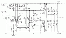
Thanks for the schematic AHT, but the one you posted is for the
555. My problem is with the 555 II which is slightly different.
I do have a schematic for it.
555. My problem is with the 555 II which is slightly different.
I do have a schematic for it.

Compuser,
I typically unsolder the RCA jacks cables and the NFB cables below the board 6 wires total. These wires are too short for you to work with the board.
Then using alligator clips connect them back temporarily. Res it on a styrofoam strip , USE A SERIES BULB ON THE MAINS and then power it up. It's works for me nicely!
K-
K-amps has a good idea. I noramally make the measurements before disassembly and fix the beast. I can do static tests for anything else. Why not measure the gain of the diff pair since it's out. Install matched pairs if the gain isn't close one these. Thermally connect them, I use heatsink grease on these and heatshrink sometimes. I hate flying leads and avoid them where possible but sometimes it's the only way. Yes, short the inputs.
Also, I wanted to know the the base voltages. If you match them they should be within a couple mV when running properly.
-Chris
Also, I wanted to know the the base voltages. If you match them they should be within a couple mV when running properly.
-Chris
Long story: Amp was assembled and rigged up with an extension for the NFB with clips. Will remain like this for the rest of the live tests. Assembled before I saw the last post. Powered up on a 100w bulb - no DC at outputs this time. (what did I change??) Without the bulb still no DC at output. There is also no BIAS at TP201/301 (TP251/351 is at 10mv) Pin 6 of IC101 rises at it warms up. Rests at 2.11VDC after about 10 mins. On IC151 it is at 5.33VDC dropping from about 5.7 after 10 mins. The diff pairs:
Base of Q101 rises very slowly to .138. (takes longer than the above 10mins) Q151 is .003. Q102/Q152 is .003.
Then I let it run an hour. There is now bias at TP201/301. (30mv so sinks are warm - I had moved the pot when there was no bias) Re-biased both sides to 10mv.
Pin 6 IC101 is 4.34. IC151 is 5.08. Base of Q101 is .002. Q102 is .003. Q151 is .006. Q152 is .003. Randomly compared voltages on left & right sides, probably in about 20 places. Basically same in both channels. I imagine it will now produce sound.
I have no idea what has caused all this. Thanks. BL
Hi Barry,
Right on! Match the diff pairs while the unit is apart. Your base readings are something I am looking at. The rise to 0.138V tells me that something is drifting. We don't want it to come back to play. The op amp output reading confirm this. If the diff pair looks like it's matched (both come to the cal mark with little or no beta cal change) then I'd be testing the other transistors in that channel.
I'm making an smt adapter for the IT-18 (smt to TO-5). Those things go leaky too.
-Chris
But where did the full DC offset go? Would this happen if I ran it for several hours? I had it at power-on at the guys house and again when I got it home and now its gone..
Hi Barry,
Okay, so why the big imbalance until the amps settles down? Time to look at the other parts. 135mV is a huge imbalance on a matched diff pair. So there is something it's trying to compensate for.
Time to go hunting.
My smt adapter works. Not bad for a device built in the seventies! Darn fiddley to use.
-Chris
Before I go further... The DC at output binding posts is gone. At power-up OR after an hour of running...it is gone. Now that the amp is cold again, powered up this morning and the Left BIAS again is zero. Base of Q201 & 301 (pins 5&6 on the board) are at 0V. (1.8v on the good channel) This will all change when it warms up.
Before I start taking out transistors and testing them, where should I be looking..on the board or on the heatsinks. (simply to save some time). Also could this drift be caused by a resistor or cap that changes value as it warms up?
Thanks BL
Before I start taking out transistors and testing them, where should I be looking..on the board or on the heatsinks. (simply to save some time). Also could this drift be caused by a resistor or cap that changes value as it warms up?
Thanks BL
Hi Barry,
Sounds like the current source (Q105). An intermittent thermal switch (S101) would do it too, but then the thermal LED should be on.
Test points are :
Q101/102 emitter should be -0.6 V ish (collector Q103).
Q108 should be biased on, collector voltage -1.8V ish.
Voltage drop across R114 / R115 - both approx 0.6V **watch out, neg. supply potential.
Voltage drop across R110 around 0.6V ** watch out, pos. supply potential.
Let me know what you find. If you think it's fixed, run it for a few days with 10R resistors across the output. 1/4W as these are "witness" resistors. We want them to burn if the offset appears. Inputs shorted.
-Chris
This is interesting, hence my I give up/where should I be looking msg earlier. Q105 was the first transistor I removed (although this was not clear in my post ) It was good. I have now tested all the transistors except Q104. This afternoon I tested D101/102. Since they were half out & I had spares, and they didnt measure the same as the spare ones (tho not far off) I repleced them AND noticed a crack (or what looked like it might be a crack) in the trace that goes from the base of Q105, D101 down to R109. Ah Ha I thought..this is it. Ran a wire to bypass the cracked trace. The closer I looked - it does seem cracked but cant meaure it so it may open up/close up under heat. Well its still not it. Still no DC at outputs but the voltages stabilize in about 5mins in what took an hour yesterday. So something is still off. There is still a similar difference (tho smaller) at IC pin6.
B
B
When the person bought this amp it had no feet and had holes in the sides where rack mount ears would have been mounted. I think it was run pretty hard in that life. There was some trace damage due to heat when I first repaired it in January. This is why I didnt want to solder/unsolder too much in that area. This current crack was in that same general area. There is a darkening of the board color in/around Q105/7/8. The socket for the bias transistor leads (talk about flying leads) that runs from the board
to the heatsink was also rebuilt because of heat damage. I will also look for more cracked traces.
B
to the heatsink was also rebuilt because of heat damage. I will also look for more cracked traces.
B
- Status
- Not open for further replies.
- Home
- Amplifiers
- Solid State
- Adcom 555 II channel failure